Etching Equipment
Etching equipment is the class of process tools that selectively removes thin films and substrate material from semiconductor wafers. Using photoresist or a hard mask as a stencil, the tool removes material only where the mask is open, turning a printed pattern into real three-dimensional structures. Etchers are among the most frequently used tools in a fab.
Also called: etch tool, etcher, dry etch system
Diagram
Dry etchers and wet etchers
Dry etchers create a plasma in a vacuum chamber and remove material in the gas phase. Ions accelerated toward the wafer make the etch directional, so dry etching can cut vertical walls and is essential for fine patterns. Reactive ion etching (RIE) is the basic principle, and tools differ mainly in how they generate the plasma: inductively coupled (ICP), capacitively coupled (CCP) or microwave sources.
Wet etchers use chemical baths or single-wafer spin processors. Wet etching is isotropic, so it is used for full-film removal, cleaning and highly selective removal rather than for defining the smallest features.
What a dry etch tool is made of
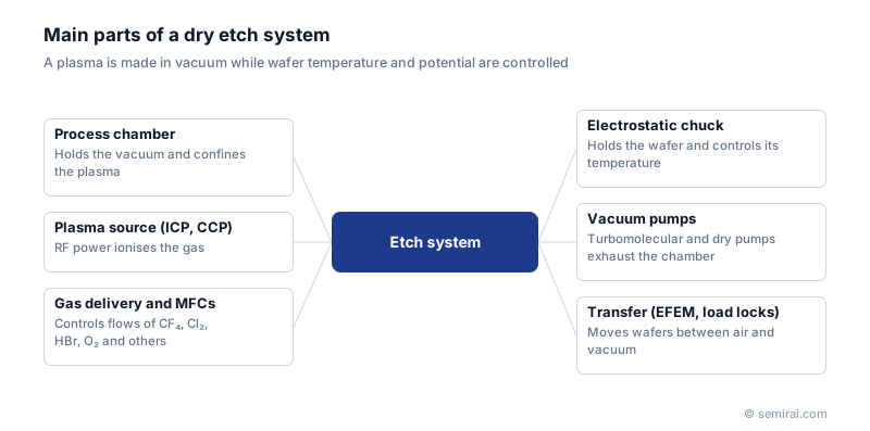
A typical system links several process chambers to a vacuum transfer module, so wafers move between steps without returning to air. Each chamber has a plasma source, a gas delivery system with mass flow controllers, an electrostatic chuck that holds the wafer and controls its temperature, an RF bias that sets ion energy, and turbomolecular and dry pumps. Load locks and an equipment front-end module pass wafers in and out of the vacuum.
Where advanced etchers are used
Etch defines many of a chip's key structures: transistor gates, fins and gate-all-around nanosheets, contact and via holes through oxide and nitride, spacer etch-back, and the very deep channel holes and slits of 3D NAND. Newer techniques such as atomic layer etching, pulsed plasmas and low-temperature (cryogenic) etching are being added to meet tighter control of shape and depth at each new node.
Japanese companies involved
- Tokyo Electron (TEL) is one of the leading global suppliers of plasma etch systems, alongside US makers Lam Research and Applied Materials.
- Hitachi High-Tech makes dry etch systems based on microwave ECR plasma, and SAMCO makes plasma etchers used for compound semiconductors, MEMS and research.
- Japanese suppliers also provide many etcher subsystems, such as electrostatic chucks from NGK Insulators and TOTO and process monitoring instruments from HORIBA.
- Tokyo Electron (TEL) · Coat/develop, etch and deposition equipment
- Hitachi High-Tech · CD-SEM metrology, defect inspection and etch systems
- SAMCO · Plasma etching, CVD and plasma cleaning equipment
- NGK Corporation · Electrostatic chucks, ceramic heaters and susceptors
- TOTO · Electrostatic chucks and fine ceramic parts
- HORIBA · Mass flow controllers and process monitoring instruments
FAQ
Why is etching done in a vacuum?
A stable plasma needs low pressure, and at low pressure ions travel to the wafer with few collisions, so they arrive almost vertically. The vacuum also lets volatile reaction products be pumped away quickly and keeps air and moisture out of the process.
How many etch steps does a modern chip need?
It varies by product, but an advanced logic or memory chip goes through many dozens of etch steps, because almost every patterned layer needs one, and multiple patterning adds more. This is why fabs install large numbers of etch chambers.
Comparisons
Related pages
Sources
Last updated: November 2, 2026