Plasma (Semiconductor Processing)
A plasma is a gas in which part of the molecules have been ionised into electrons and positive ions, often called the fourth state of matter. In semiconductor manufacturing, low-pressure plasmas driven by RF or microwave power supply reactive radicals and directional ions to the wafer, and they are the basis of dry etching, plasma CVD, ashing and chamber cleaning.
Also called: process plasma, low-temperature plasma
Diagram
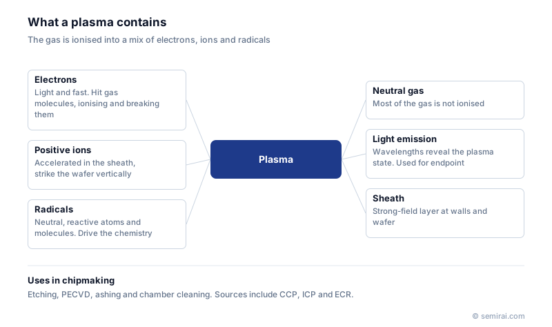
What is inside a process plasma
Process plasmas are weakly ionised: most of the gas stays neutral, and only a small fraction is ionised. Electrons absorb energy from the applied field and become very hot, with energies of a few electronvolts, while ions and neutral gas stay near room temperature. This is why such plasmas are called low-temperature or non-equilibrium plasmas, and why they can drive chemistry without heating the wafer much.
Collisions between energetic electrons and gas molecules create ions, and also break molecules into radicals: neutral fragments such as fluorine or chlorine atoms that react strongly with surfaces. Excited species emit light, whose spectrum reveals what the plasma contains. Next to every surface a thin sheath forms, a region with a strong electric field that accelerates positive ions straight onto the wafer.
Where plasma is used
In dry etching, radicals react with the film to form volatile products and ions arriving vertically make the etch directional, so patterns can be cut with straight walls. In PECVD and plasma-enhanced ALD, the plasma breaks down precursors so films grow at low temperature. Oxygen plasma ashing strips photoresist, and fluorine-based plasmas clean deposits from chamber walls between wafers. Plasmas are also used to modify surfaces, for example before bonding. Changes in the light emitted by the plasma are widely used to detect the endpoint of an etch.
How plasmas are generated
A capacitively coupled plasma (CCP) is driven by RF voltage between two parallel electrodes. It is simple and gives high ion energy; dual-frequency CCPs, with one frequency mainly setting plasma density and another the ion energy, dominate dielectric etching. An inductively coupled plasma (ICP) is driven by a coil antenna and reaches higher density at lower pressure, with a separate bias supply on the wafer to set ion energy; it is common in silicon and metal etching. Microwave sources, including electron cyclotron resonance (ECR) plasmas, are another way to reach high density at low pressure.
Plasmas can also harm devices. Energetic ions, ultraviolet light and charge build-up can create defects in gate dielectrics, so pulsed plasmas, remote plasmas and low-energy techniques such as atomic layer etching are used for sensitive steps.
Japanese companies involved
- Tokyo Electron makes plasma etch and deposition systems, including capacitively coupled etchers for dielectric films.
- Hitachi High-Tech makes plasma etch systems based on microwave ECR plasma sources.
- Kyosan Electric Manufacturing makes power supplies used in semiconductor and flat-panel display equipment.
- Hitachi High-Tech · CD-SEM metrology, defect inspection and etch systems
- Tokyo Electron (TEL) · Coat/develop, etch and deposition equipment
- Kyosan Electric Manufacturing · Power supplies for semiconductor and FPD equipment
FAQ
Why does semiconductor processing use low-pressure plasma?
At low pressure electrons travel far enough between collisions to gain the energy needed for ionisation, and ions cross the sheath with few collisions, so they arrive at the wafer nearly vertically. That directionality is what makes anisotropic etching possible.
What is the difference between a radical and an ion?
A radical is an electrically neutral, chemically reactive fragment of a molecule; it moves randomly and does most of the chemical work. An ion carries charge, so it can be accelerated by the sheath field and steered toward the wafer, delivering energy in one direction.
What is a remote plasma?
In a remote plasma source the plasma is created away from the wafer, and only long-lived radicals flow into the process chamber. Ions and ultraviolet light are largely kept away, so it is used for gentle processes such as chamber cleaning, photoresist stripping and isotropic etching.
Related pages
Sources
Last updated: November 2, 2026