Latch-up
Latch-up is a failure in which a parasitic thyristor, a pnpn structure formed unintentionally inside CMOS circuits, turns on and lets a large current flow continuously between the power supply and ground. Once triggered, the current keeps flowing until power is removed, and it often destroys the chip by melting wires or burning the silicon.
Also called: CMOS latch-up, single-event latch-up
Diagram
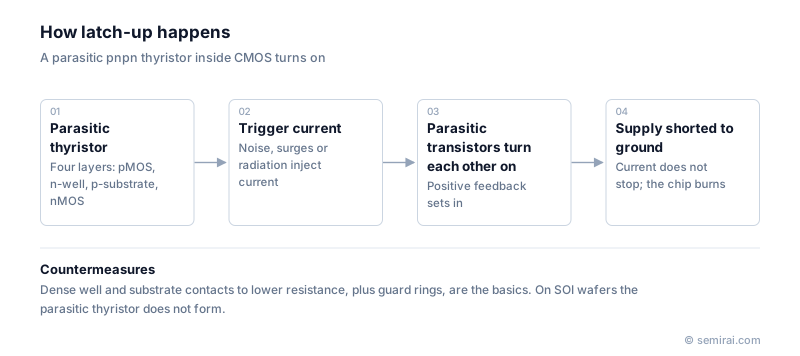
Where the parasitic thyristor comes from
The cause lies in the CMOS structure itself. When a pMOS transistor in an n-well sits next to an nMOS transistor in the p-type substrate, the diffusions, well and substrate form a parasitic pnp transistor and a parasitic npn transistor. The collector of each feeds the base of the other, creating a positive feedback loop.
If the product of the two transistors' current gains exceeds one, a small trigger is enough to switch the loop on, and it then holds itself on. The resistances of the well and substrate determine how easily the trigger current turns the transistors on.
Triggers and countermeasures
Latch-up is triggered by current injected into the well or substrate. Typical causes are signals at an I/O pin that go above the supply or below ground, transients during power-up, ESD events, and charge generated by cosmic rays or other radiation, which is called single-event latch-up.
Layout is the first line of defence. Placing well and substrate contacts (taps) densely lowers the base resistance of the parasitic transistors, keeping enough distance between pMOS and nMOS reduces their gain, and guard rings collect injected current before it can trigger the loop. Process choices help as well: on silicon-on-insulator (SOI) wafers each transistor is fully isolated by oxide, so the parasitic thyristor does not form and latch-up cannot occur in the usual way.
Japanese companies involved
- Toshiba Electronic Devices & Storage publishes application guidance on preventing latch-up when using its CMOS logic ICs.
- Toshiba Electronic Devices & Storage · Power MOSFETs, IGBTs and discrete semiconductors
- ESPEC · Environmental and reliability test chambers
FAQ
How is latch-up tested?
JEDEC JESD78 defines the test. Current, typically up to about plus or minus 100 mA, is injected into each pin, and supplies are driven above their maximum rating, while the supply current is monitored. A device fails if the current rises abnormally and stays high.
Can a chip recover from latch-up?
Sometimes. If the current is limited by the power supply or a protection circuit and power is cycled quickly, the device may survive. Often, though, the current is large enough to damage wiring or junctions permanently.
Comparisons
Related pages
- ESD Test (HBM / CDM)
- CMOS (Complementary Metal-Oxide-Semiconductor)
- SOI (Silicon on Insulator)
- Shallow Trench Isolation (STI)
- Failure Analysis (FA)
- Bipolar Junction Transistor (BJT)
- Bulk Silicon
- Soft Error
- Final test equipment
- Advantest 7038 System-Level Test System
- Advantest T2000
- DISCO DIS100
- Tokyo Electron (TEL) Prexa™ SDP
Sources
Last updated: November 2, 2026