High Energy Ion Implantation
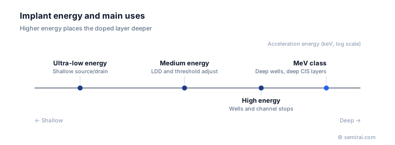
High energy ion implantation accelerates ions to energies from several hundred keV to several MeV (million electron volts) to form doped layers deep below the silicon surface, down to several micrometres. Because the depth at which ions stop rises with energy, deep layers need high energies and dedicated implanters.
Also called: MeV implantation, high-energy implant
Diagram
Where it is used
A key use is the CMOS well, the doped region on which transistors are built. A retrograde well, with its highest concentration deep below the surface, improves resistance to latch-up and can replace the long high-temperature drive-in that used to form wells.
In CMOS image sensors, high-energy implants form deep photodiodes and the deep isolation layers between neighbouring pixels. Deep photodiodes collect more of the long-wavelength light that penetrates far into silicon, and deep isolation stops charge from leaking into neighbouring pixels and mixing colours. Power semiconductors also use high-energy implants for deep doped layers.
How the ions are accelerated
Reaching MeV energies needs special accelerators. Tandem machines apply a high voltage twice by changing the charge of the ion halfway through, and linear accelerators (linacs) add energy step by step with radio-frequency fields.
Deep implants also need thick masks, because the ions must be stopped where no doping is wanted; thick photoresist or hard masks are used. Accurate energy control and careful control of channeling are essential to keep the depth reproducible.
Japanese companies involved
- Sumitomo Heavy Industries Material Solutions (formerly SMIT) and Nissin Ion Equipment make ion implanters, the tools whose acceleration energy determines how deep a doped layer can be placed.
- Nissin Ion Equipment · Ion implanters
- Sumitomo Heavy Industries Material Solutions (formerly SMIT) · Ion implanters
FAQ
Why do CMOS image sensors need high-energy implants?
Red and near-infrared light penetrates several micrometres into silicon before it is absorbed. Photodiodes and pixel isolation must reach that depth to collect the signal and keep it in the right pixel, and only high-energy implants can dope that deep without long, hot diffusion steps.
How do high-energy implanters differ from standard ones?
Standard implanters work from a few keV to a few hundred keV with a single acceleration stage. High-energy implanters add tandem or linac accelerators to reach MeV levels, and they need more shielding and more careful beam tuning.
Related pages
Sources
Ion implantation and thermal processing terms
Last updated: November 2, 2026