Diamond Semiconductor
A diamond semiconductor uses single-crystal diamond, carbon atoms bonded in the diamond lattice, as a semiconductor material. Its bandgap of about 5.5 eV is far larger than that of SiC or GaN, and its breakdown field and thermal conductivity are exceptionally high, so it is studied as a candidate for future power and harsh-environment devices.
Also called: diamond power device, synthetic diamond semiconductor
Diagram
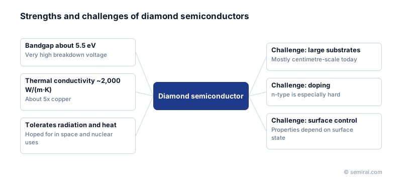
Why diamond is attractive
Diamond combines several extreme properties. The wide bandgap allows very high breakdown fields, and its thermal conductivity of about 2,000 W/(m·K) is roughly five times that of copper and several times that of SiC, among the highest of any material. It is also highly resistant to radiation and high temperature.
These properties point to applications in power conversion, high-frequency amplifiers and electronics that must work in space, around nuclear reactors or in other harsh environments. Device crystals are grown by microwave plasma chemical vapour deposition (CVD), in which methane and hydrogen are broken down in a plasma and carbon is deposited on a substrate. Natural gem diamond is not used.
What holds diamond back
Three challenges stand in the way of commercial devices. First, large single-crystal substrates are hard to make; current substrates are centimetre-scale, far from the wafer sizes used for silicon or SiC. Second, doping is difficult. Boron gives p-type material, but n-type doping with phosphorus produces donors that need a large energy to release their electrons, so n-type layers conduct poorly at room temperature. Third, device characteristics depend strongly on the surface state, which must be carefully controlled.
Transistor operation has been demonstrated, and work continues on larger substrates and better doping. Substrate size and doping are widely seen as the keys to mass production.
Japanese companies involved
- The National Institute of Advanced Industrial Science and Technology (AIST) and several Japanese universities have long-running diamond device research programmes, including substrate growth and transistor demonstrations.
- Sumitomo Electric Industries produces synthetic single-crystal diamond, a material relevant to diamond substrates.
- Sumitomo Electric Industries (compound semiconductors) · SiC epitaxial wafers and GaAs and InP substrates
FAQ
When will diamond semiconductors be commercialised?
They are still in research and development. Mass production needs large substrates and reliable doping. Early use is expected in niche applications that value radiation or heat tolerance, with general power devices further away.
Is diamond also used with other semiconductors?
Yes. Because of its thermal conductivity, diamond is studied and used as a heat spreader or substrate under hot devices such as GaN high-frequency transistors, to carry heat away from the active region.
Related pages
- Wide Bandgap Semiconductor (WBG)
- Band Gap
- Silicon Carbide (SiC)
- Gallium Nitride (GaN)
- Breakdown Voltage
- Donor and Acceptor
- Semiconductor materials (wafers and substrates)
- Sumitomo Electric Industries (compound semiconductors) GaAs and InP substrates
- Shin-Etsu Chemical 300 mm silicon wafers
- SUMCO Polished wafers (PW)
Sources
Last updated: November 12, 2026