Wide Bandgap Semiconductor (WBG)
A wide bandgap (WBG) semiconductor is a material whose bandgap is much wider than that of silicon (about 1.1 eV). The main examples are silicon carbide (about 3.26 eV for 4H-SiC) and gallium nitride (about 3.4 eV). Their high breakdown field lets power devices block the same voltage with far lower losses.
Also called: WBG, wide-bandgap semiconductor, wide-gap semiconductor
Diagram
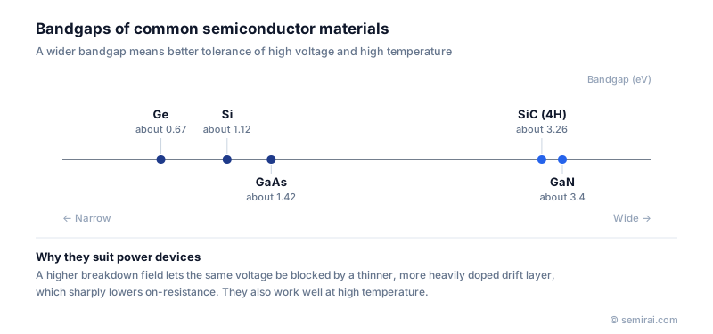
Why a wide bandgap helps
The first consequence is a higher critical electric field. SiC withstands roughly ten times the field of silicon before avalanche breakdown, so a drift layer that blocks a given voltage can be about one-tenth as thick and much more heavily doped. Because the drift layer dominates on-resistance in high-voltage devices, the resistance at the same voltage rating drops dramatically.
The second is high-temperature operation. With a wide gap, heat creates very few electron-hole pairs, so the intrinsic carrier concentration stays low and the device keeps blocking at temperatures where silicon would leak. The third is fast switching: a thin drift layer stores little charge, so turn-off is quick and switching loss stays low at higher frequencies. Higher frequency allows smaller transformers, inductors and capacitors, which is why GaN chargers are so compact.
SiC, GaN and the next materials
SiC is used mostly as vertical MOSFETs and Schottky diodes from about 650 V to several kilovolts, in electric-vehicle inverters, chargers, solar inverters and railways. GaN is usually grown as a thin layer on silicon or SiC substrates and made into lateral high-electron-mobility transistors (HEMTs), which suit 100 V to 650 V power supplies and radio-frequency amplifiers.
Gallium oxide (Ga₂O₃, about 4.8 eV) and diamond (about 5.5 eV) have even wider gaps and are being researched for very high voltages, but they face problems such as poor thermal conductivity or the difficulty of p-type doping.
Manufacturing challenges
SiC cannot be pulled from a melt like silicon; crystals are grown by sublimation at well above 2,000 °C, which is slow and prone to defects, so substrates are expensive and the industry is moving from 150 mm to 200 mm wafers. GaN-on-silicon is cheaper but makes vertical high-voltage devices hard, which limits its voltage range.
Japanese companies involved
- ROHM and Mitsubishi Electric make SiC power devices and modules, and Japanese research has played a large part in early SiC and gallium oxide development.
- ROHM · SiC and silicon power devices, analog ICs
- Mitsubishi Electric (power devices) · IGBT and SiC power modules, RF and optical devices
FAQ
Is GaAs a wide bandgap semiconductor?
Usually not. Gallium arsenide has a bandgap of about 1.42 eV, a little wider than silicon, and is valued for its high electron mobility in RF and optoelectronic devices. The term wide bandgap normally refers to materials around 3 eV and above.
Why is the SiC gate oxide a concern?
The SiC-to-silicon dioxide interface has more traps than silicon's, which lowers channel mobility and can shift the threshold voltage over time. Improved nitridation anneals and trench gate designs have reduced the problem, but gate reliability is still checked carefully.
Do wide bandgap devices need special drivers?
Often yes. They switch so fast that layout inductance causes overshoot and noise, and some require specific gate voltages. Drivers, packages and circuit boards are therefore designed together with the device.
Comparisons
Related pages
Sources
Last updated: November 2, 2026