Silicon Carbide (SiC)
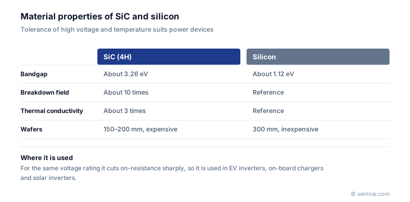
Silicon carbide (SiC) is a compound semiconductor of silicon and carbon, both group IV elements. Its 4H polytype has a bandgap of about 3.26 eV, a breakdown field roughly ten times that of silicon and about three times silicon's thermal conductivity, which makes it the main material for power MOSFETs and diodes that switch high voltages efficiently.
Also called: SiC, 4H-SiC
Diagram
Why SiC suits power devices
A power transistor must block high voltage when off and conduct with little loss when on. Blocking voltage is held by a lightly doped drift layer. Because SiC withstands about ten times the electric field of silicon, the drift layer for a given voltage can be about a tenth as thick and much more heavily doped, so its resistance is far lower. That lets SiC MOSFETs replace silicon IGBTs at 650 V to 1,700 V and above with lower switching loss and higher operating frequency.
The wide bandgap also keeps leakage low at high temperature, and the high thermal conductivity helps remove heat. Together these allow smaller cooling systems and passive components. The main applications are traction inverters and on-board chargers in electric vehicles, fast chargers, solar and storage inverters, industrial drives and railway systems.
Making SiC wafers
SiC does not melt at practical pressures, so the Czochralski pulling used for silicon is impossible. Single crystals are grown by physical vapour transport (PVT): SiC powder sublimes at well above 2,000 °C and recondenses on a seed crystal. Growth is slow and the boules are short, so substrates are much more expensive than silicon. Diameters have moved from 100 mm to 150 mm, and 200 mm is entering production. Crystal defects such as micropipes, basal plane dislocations and stacking faults remain the main quality issue, and an epitaxial SiC layer is grown on each substrate to form the device's drift region.
How SiC processing differs from silicon
Dopants hardly diffuse in SiC, so all doping is done by ion implantation, often with the wafer heated to several hundred degrees to limit damage. Activating the dopants needs annealing at 1,600 °C or more. The thermal oxide grown on SiC has a poorer interface than on silicon, which lowers channel mobility, so gate oxides are typically annealed in nitric oxide (NO) or nitrous oxide (N₂O) to passivate it. SiC is also very hard, which slows wafer slicing, grinding and dicing.
Japanese companies involved
- ROHM makes SiC MOSFETs and Schottky diodes and, through its subsidiary SiCrystal, SiC substrates.
- Sumitomo Electric and Resonac produce SiC epitaxial wafers for power-device makers.
- Mitsubishi Electric uses SiC power modules in railway and industrial equipment.
- ROHM · SiC and silicon power devices, analog ICs
- Resonac · CMP slurries, packaging materials and SiC epitaxial wafers
- Mitsubishi Electric (power devices) · IGBT and SiC power modules, RF and optical devices
- Sumitomo Electric Industries (compound semiconductors) · SiC epitaxial wafers and GaAs and InP substrates
FAQ
What is the difference between SiC and GaN?
Both are wide-bandgap semiconductors. SiC is grown as bulk vertical devices and dominates high-voltage, high-power uses such as EV inverters. GaN is usually grown as thin layers on silicon or other substrates and used in lateral transistors that switch very fast at lower voltages, such as compact chargers and RF amplifiers.
What do 4H and 6H mean?
SiC exists in many crystal stackings called polytypes. The number gives how many layers repeat in the stacking sequence and H means hexagonal. 4H-SiC has the highest electron mobility and a wide bandgap, so it is the polytype used for power devices.
Why are SiC devices more expensive than silicon ones?
Substrates are grown slowly by sublimation, wafers are smaller, defects reduce yield, and the material's hardness and high process temperatures need specialised equipment. Cost per amp has been falling as wafers grow to 200 mm and production volumes rise.
Comparisons
Related pages
Sources
Last updated: November 2, 2026