Footprint
Footprint is the floor area an object occupies. In a semiconductor fab, a tool's footprint is the cleanroom floor space it takes up, and it is a key equipment specification. In electronics design the word also means the land pattern for a component on a circuit board, and in environmental use the carbon footprint.
Also called: tool footprint, equipment footprint
Diagram
Why footprint matters
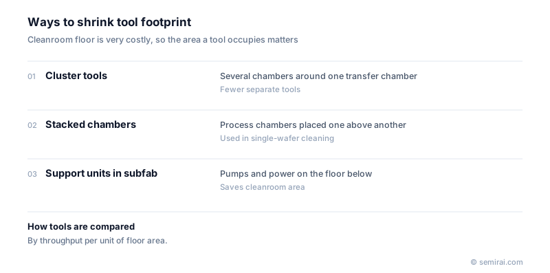
Cleanroom floor space is expensive to build and to run, because it comes with filtered air, temperature and humidity control, vibration-resistant structure and utilities. How much production capacity fits into a given building decides the return on the fab investment.
Tools are therefore compared not only by throughput in wafers per hour but by throughput per unit of floor area. Tool makers reduce footprint with cluster tools, which group several process chambers around one transfer chamber, by stacking chambers vertically, as in many single-wafer cleaning tools, and by designs that need less service space around the tool.
What is counted
A realistic footprint includes more than the tool body. It includes the service area needed to open panels and replace parts, the load ports at the front and their relation to transport aisles, and the support equipment in the subfab below, such as vacuum pumps, power supplies and abatement units.
When a fab is designed, planners add up each tool's footprint and service area to set the size and layout of the cleanroom, and leave margin for adding or replacing tools later.
Japanese companies involved
- Tokyo Electron and other Japanese tool makers design multi-chamber and stacked-chamber platforms to raise throughput per unit of floor area.
- Tokyo Electron (TEL) · Coat/develop, etch and deposition equipment
FAQ
What does footprint mean in general?
Literally a footprint is a mark left by a foot. The word is used for the area something occupies, the land pattern of an electronic component on a printed circuit board, and the total greenhouse gas emissions of an activity, depending on the field.
Why are tools compared by throughput per floor area?
Because floor space, not just tool price, is a scarce resource in a fab. A tool that is slightly slower but much smaller can give more wafers per square metre of cleanroom, which may make it the better choice.
Related pages
Sources
Last updated: November 2, 2026