Process Chamber
A process chamber is the sealed vessel inside a semiconductor manufacturing tool in which a wafer is actually processed, for example by deposition, etching or annealing. Most chambers are held under vacuum and contain a wafer stage such as an electrostatic chuck, a showerhead that distributes gas, electrodes or coils that form plasma, and an exhaust port with pressure control.
Also called: chamber, reaction chamber, process module
Diagram
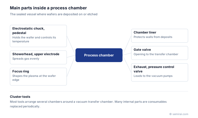
What is inside a chamber
The wafer sits on a stage that holds it and sets its temperature: an electrostatic chuck in most etch tools, or a heated pedestal or susceptor in deposition tools. Above it, a showerhead spreads process gas evenly and often doubles as the upper electrode. Plasma chambers add RF electrodes or an inductive coil, and a focus ring around the wafer edge shapes the plasma there. A gate valve connects the chamber to the transfer system, and the exhaust leads through a pressure-control valve to the vacuum pumps.
Chamber parts face corrosive gases and plasma, so they are made of resistant materials: anodised aluminium, yttria-coated surfaces, quartz, and ceramics such as alumina and silicon carbide.
Cluster tools and batch tubes
Most modern equipment is a cluster tool: several process chambers and load locks are arranged around a vacuum transfer chamber with a robot in the middle. Wafers move from step to step without seeing air, which prevents oxidation and contamination between steps, and the chambers work in parallel to raise throughput. Most such chambers are single-wafer. Oxidation, diffusion and LPCVD furnaces are the main exception: they process around a hundred or more wafers at once in a vertical quartz tube.
Cleaning, consumables and matching
Every run leaves films and reaction products on the walls and parts. If they flake off, they land on wafers as particles. Chambers are therefore cleaned in place between wafers or lots, for example with a plasma of fluorine-containing gas, and periodically opened for preventive maintenance in which liners, focus rings, showerheads and other consumable parts are replaced or cleaned.
A fab may run the same process in dozens of identical chambers, and each must give the same result. Keeping etch rate, film thickness and uniformity aligned across chambers, called chamber matching, is a routine but demanding part of high-volume manufacturing.
Japanese companies involved
- Tokyo Electron builds single-wafer etch and deposition tools and multi-chamber platforms, as well as batch furnaces.
- Kokusai Electric makes vertical batch furnaces whose quartz process tubes handle oxidation, diffusion, LPCVD and ALD.
- Mirapro and Marumae supply precision-machined vacuum chambers, bellows and other parts to equipment makers.
- Tokyo Electron (TEL) · Coat/develop, etch and deposition equipment
- Kokusai Electric · Batch deposition, diffusion and ALD equipment
- Mirapro · Bellows, vacuum piping and vacuum components
- Marumae · Precision-machined vacuum parts for equipment
FAQ
Why must chambers be cleaned so often?
Deposits build up with every wafer. Thick deposits crack and shed particles, and they also change the chamber's surfaces, which shifts plasma conditions and process results over time. Regular in-situ cleaning keeps the walls in a steady state, and scheduled maintenance removes what cleaning cannot.
What is chamber seasoning?
After a wet clean or parts replacement, the fresh walls behave differently from walls that have seen many wafers. Engineers run dummy wafers or a deposition step to coat the walls until results stabilise, then qualify the chamber with test wafers before it returns to production.
Related pages
Sources
Last updated: November 2, 2026