Hard Mask
A hard mask is a thin film, usually inorganic or carbon-based, used instead of photoresist or beneath it as the mask for etching. Resist is relatively weak against plasma etching, so for deep etches or those needing high selectivity, the resist pattern is first transferred into a more durable hard mask, which then protects the target layer.
Also called: hardmask, HM
Diagram
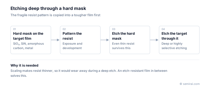
Why hard masks are needed
As features shrink, resist films must become thinner to avoid pattern collapse and to stay within the depth of focus. A thin resist can be consumed before a deep etch finishes. Inserting a hard mask breaks the job into steps: the thin resist only has to survive a short etch into the hard mask, and the hard mask survives the long etch into the target layer.
Common materials include silicon oxide, silicon nitride, amorphous carbon and spin-on carbon, titanium nitride and other metals or metal oxides. They differ in etch resistance, optical absorption, film stress and ease of removal, and are combined to suit each process.
Multilayer stacks and multi-patterning
A typical stack is a thick carbon layer, a thin silicon-containing layer and the resist on top. Each layer is etched with chemistry that attacks it but not the layer above, so the pattern is relayed downward with high fidelity. Very deep etches, such as memory holes in 3D NAND, use thick amorphous carbon or metal-containing hard masks.
In self-aligned double and quadruple patterning, hard masks form the cores on which spacers are deposited, and the spacers then become the mask. These schemes depend on precise deposition, often by atomic layer deposition, and highly selective etching. Metal hard masks such as titanium nitride are widely used in back-end interconnect patterning.
Japanese companies involved
- JSR supplies spin-on underlayer materials used in multilayer resist and hard mask stacks.
- ULVAC makes sputtering equipment used to deposit metal hard mask films, and Tokyo Electron makes deposition and etch equipment used to form and open hard masks.
- ULVAC · Vacuum deposition (sputtering) equipment and vacuum pumps
- Tokyo Electron (TEL) · Coat/develop, etch and deposition equipment
- JSR · Photoresists and semiconductor materials
FAQ
Why is it called a hard mask?
Because the film is harder, in the sense of more etch-resistant, than photoresist, which is a soft organic polymer. The name contrasts it with the soft mask formed by resist.
Is the hard mask removed afterwards?
Usually yes, by a selective etch or ashing for carbon films. Some hard masks, such as nitride layers, are left in place when they also serve as an etch stop or a polish stop in later steps.
What is spin-on carbon?
A carbon-rich polymer applied by spin coating rather than by deposition. It fills topography and planarises the surface, giving a flat base for lithography, and acts as the bottom layer of a trilayer stack.
Related pages
Sources
Last updated: November 2, 2026