Sheet Resistance (Rs)
Sheet resistance (Rs) is the resistance of a thin conductive layer measured along its surface, expressed in ohms per square (Ω/sq). It equals the material's resistivity divided by the layer thickness, and any square of the layer has the same resistance whatever its size, which makes it a convenient single number for diffused, implanted and metal films.
Also called: four-point probe measurement, ohms per square
Diagram
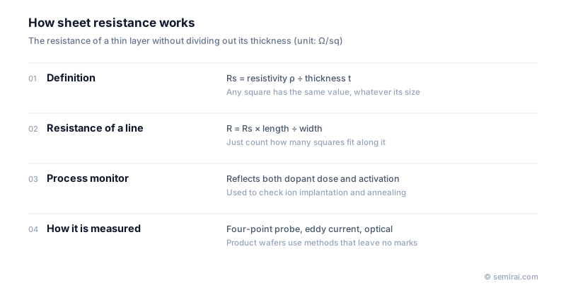
Why the unit is ohms per square
The resistance of a rectangular strip of film is R = ρL / (Wt), where ρ is resistivity, L the length, W the width and t the thickness. Grouping ρ/t into one quantity gives R = Rs × L/W. A square has L/W = 1, so every square of the film, large or small, has a resistance of exactly Rs. To estimate the resistance of a line, a designer simply counts how many squares fit along it.
The unit is strictly ohms, but writing Ω/sq signals that the value refers to a film and not to a single resistor. Rs is used for doped layers in silicon, polysilicon gates, silicides, barrier metals and copper interconnect films, wherever current flows in the plane of the layer.
How it is measured
The standard method is the four-point probe. Four needles are placed in a line with equal spacing; a current is passed through the outer two and the voltage is measured across the inner two. Because almost no current flows in the voltage probes, contact resistance at the needles drops out of the result. For a thin layer that is large compared with the probe spacing, Rs = (π / ln 2) × V/I, or about 4.53 × V/I; smaller or irregular samples need geometric correction factors.
The needles leave marks, so four-point probing is done on monitor wafers rather than product wafers. For product wafers, fabs use non-contact methods: eddy-current gauges for metal films, and optical tools that detect thermal waves or changes in reflectance caused by excited carriers. These give relative maps of implant dose and damage across the wafer without touching it.
Where it matters in manufacturing
Sheet resistance is the everyday check for ion implantation and annealing. How much of the implanted dopant became electrically active, and how far it diffused, are hard to measure separately, but both show up in a single Rs value. Fabs therefore run monitor wafers with each implant or anneal recipe and track Rs and its uniformity on control charts. In the back end of line, Rs of copper, barrier and silicide films is compared with the values assumed in circuit design.
Japanese companies involved
- Japanese instrument makers supply four-point probe and eddy-current resistivity systems used in wafer and process monitoring, alongside the optical and electrical metrology tools of US and Israeli suppliers.
FAQ
How is sheet resistance converted to resistivity?
Multiply it by the layer thickness: ρ = Rs × t. For a 100 nm film with Rs of 0.2 Ω/sq, resistivity is 2 µΩ·cm. For a diffused layer whose doping varies with depth, the result is an average, so profile methods such as SIMS or spreading resistance are needed to see the depth distribution.
Why does sheet resistance fall after annealing an implant?
As implanted, many dopant atoms sit off lattice sites and the crystal is damaged, so few carriers are available. Annealing repairs the damage and moves dopants onto lattice sites where they release carriers, so Rs drops. A higher-than-expected Rs after anneal points to low activation, a dose error or an anneal temperature problem.
What is the van der Pauw method?
A four-terminal technique that measures sheet resistance of a sample of arbitrary shape by placing contacts at its edge and combining two resistance readings. It is common in research and in test structures, and with a magnetic field it also gives carrier concentration and mobility through the Hall effect.
Related pages
Sources
Inspection and metrology terms
Last updated: November 2, 2026