Lapping
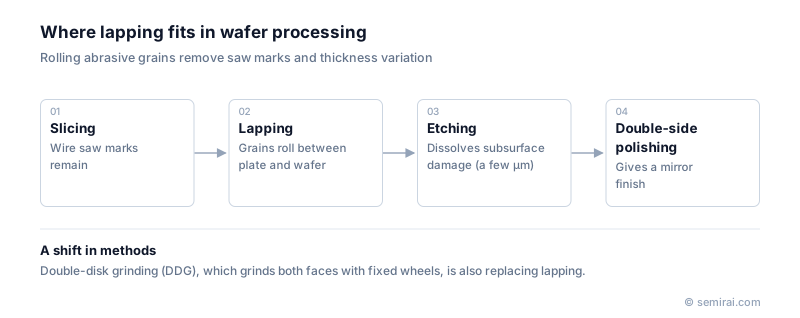
Lapping is a flattening process in which a slurry of loose abrasive grains is fed between a rotating plate and the wafer, and the rolling grains remove material. In wafer manufacturing it follows slicing: it removes saw marks and thickness variation and produces a flatness good enough to pass to etching and polishing.
Also called: free-abrasive lapping, double-side lapping
Diagram
How a lapping machine works
A typical machine holds wafers in thin carriers between an upper and a lower plate. A planetary gear system makes the carriers rotate and orbit while the plates press on both faces. The slurry contains alumina or silicon carbide grains a few micrometres in size. Because the grains are not fixed, they roll randomly across the surface and remove material by tiny fractures.
Lapping removes a large allowance quickly and gives good flatness. The cost is a damaged layer several micrometres deep beneath the surface, created as grains are pressed into it. This layer would harm devices, so chemical etching and mirror polishing must remove it completely.
Lapping vs double-side grinding
Many lines now use double-disk grinding (DDG), with fixed abrasive wheels on both faces, in place of lapping. Grinding needs no slurry handling, is faster and leaves a shallower damaged layer, so the sequence becomes slice, grind, etch and polish. Lapping still has strengths in producing flatness, and both approaches are in use.
Lapping differs from chemical mechanical polishing (CMP), which comes later. CMP combines a chemical reaction with very fine abrasives to give a damage-free mirror surface but removes material slowly.
Japanese companies involved
- SpeedFam and Hamai Industries make lapping and double-side polishing machines for silicon and other wafers.
- Fujimi Incorporated supplies lapping abrasives and polishing slurries used in wafer production.
- SpeedFam · Wafer polishing and lapping equipment
- Hamai Industries · Lapping and polishing machines for wafers
- Fujimi Incorporated · CMP slurries and polishing materials
FAQ
Why not polish the wafer directly after slicing?
Polishing removes material very slowly. Saw marks and thickness differences after slicing are too large to polish away economically, so a faster flattening step comes first and polishing only finishes the surface.
What decides the result of lapping?
The combination of machine, plate flatness, abrasive type and size, slurry supply, carrier material and pressure. Together they set the final flatness, the depth of damage and the throughput.
Related pages
- Wire Saw
- Wafer Flatness (TTV / SFQR / GBIR)
- CMP (Chemical Mechanical Polishing)
- Silicon Wafer Manufacturing
- CMP Slurry
- Polishing Pad (CMP Pad)
- Removal Rate (Preston Equation)
- Abrasive
- Wafer polishing and edge grinding equipment
- SpeedFam FAM59SPAW / FAM50SPAW
- SpeedFam UH-I-8100 / UH-I-8800
- SpeedFam WIFG-300
- DISCO DFP8141
Sources
Last updated: November 13, 2026