Silicon Ingot
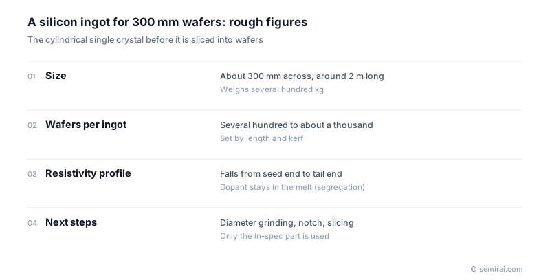
A silicon ingot is the cylindrical single crystal of silicon from which wafers are sliced. It is grown from high-purity polysilicon by the Czochralski or float zone method. An ingot for 300 mm wafers is about 300 mm across and around two metres long, weighs several hundred kilograms and yields hundreds of wafers.
Also called: single-crystal silicon ingot, silicon boule
Diagram
The shape of a grown crystal
In the Czochralski method the crystal is pulled from a melt held at about 1,420 °C, at a rate on the order of a millimetre per minute. Growth goes through five stages: seeding, necking (a thin neck that removes dislocations), the shoulder (widening to the target diameter), the body (constant diameter) and the tail (narrowing so the crystal can leave the melt without a thermal shock). How well each stage is controlled decides how uniform the crystal is.
Properties change along the length of the ingot. Dopants such as boron and phosphorus prefer to stay in the melt (segregation), so their concentration in the melt rises as growth continues, and the resistivity of the crystal falls from the seed end to the tail end. The oxygen content also changes as the melt level drops. Because of this axial profile, only part of each ingot meets a given specification.
From ingot to slices
After growth, resistivity, oxygen, defect density and carrier lifetime are measured and the ingot is sorted. It is ground to an exact diameter, notched to mark the crystal orientation, cut into blocks and sent to slicing. The out-of-specification head and tail are cut off and remelted.
Larger ingots give more chips per wafer, but they are heavier and harder to grow: crucible strength, melt convection and the stiffness of the pulling mechanism all become harder to manage. This, together with the cost of re-equipping fabs, is why the move from 300 mm to 450 mm wafers has not happened.
Japanese companies involved
- Shin-Etsu Chemical and SUMCO grow silicon ingots for their wafer businesses.
- Ferrotec supplies quartz and silicon parts and other consumables used in semiconductor and crystal-growth equipment.
- Shin-Etsu Chemical · Silicon wafers, photoresists and photomask blanks
- SUMCO · Silicon wafers
- Ferrotec · Quartz, silicon and ceramic parts for equipment; thermoelectric modules
FAQ
How many wafers does one ingot give?
The number is roughly the usable length divided by the sum of wafer thickness, saw kerf and polishing allowance. Reducing kerf loss therefore increases output directly without extra crystal growth.
Why is the ingot ground after growth?
The as-grown diameter wanders slightly and is a little larger than the target. Grinding the outside makes the diameter exact and round, which wafer handling equipment depends on, and the orientation notch is cut at the same stage.
Related pages
Sources
Last updated: November 13, 2026