Metal Contamination
Metal contamination is the presence of trace metal impurities, such as iron, copper, nickel, aluminium or sodium, on a wafer surface or inside the silicon crystal, where they degrade device behaviour. Unlike particles, which sit on the surface, metals bond at atomic level or diffuse into the silicon, so they are invisible and hard to remove.
Also called: metallic contamination, trace metal contamination
Diagram
Effects on devices
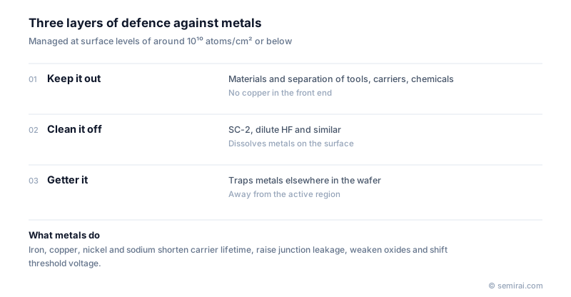
Iron and copper create deep energy levels in silicon that shorten minority carrier lifetime and increase junction leakage. Metals taken into the gate oxide lower its breakdown strength, known as gate oxide integrity (GOI). Mobile ions such as sodium move under electric fields and shift the threshold voltage over time.
In image sensors the result is higher dark current; in power devices it shows up as spread in characteristics. For these reasons fabs typically manage surface metal levels on the order of 10¹⁰ atoms/cm² or lower.
Sources and control
Metals come from many places: trace levels in chemicals, ultrapure water and gases; parts of piping and valves; sputtering of chamber parts in implant and deposition tools; CMP slurries; and contact during handling. Control works in three layers. First, keep metals out with high-purity materials and plastic piping. Second, remove them by cleaning, for example SC-2 (hydrochloric acid and hydrogen peroxide) or dilute HF. Third, make the remainder harmless by gettering, which traps metals at defect sites away from the active device region.
Total reflection X-ray fluorescence (TXRF) measures surface metals directly, and vapour phase decomposition with ICP mass spectrometry (VPD-ICP-MS) reaches lower levels. Fabs run monitor wafers through tools regularly, and a tool that exceeds its limit is taken down for maintenance.
Japanese companies involved
- Rigaku makes TXRF instruments used to measure metal contamination on wafer surfaces.
- Stella Chemifa supplies high-purity hydrofluoric acid, and Kurita Water Industries supplies ultrapure water systems; both help keep metals out of process fluids.
- SCREEN Holdings · Wafer cleaning, coat/develop and inspection equipment
- Kurita Water Industries · Ultrapure water systems and wastewater treatment
- Rigaku · X-ray metrology and thermal analysis
- Stella Chemifa · High-purity hydrofluoric acid and fluorine chemicals
FAQ
How is metal contamination different from particle contamination?
A particle is a physical object on the surface that can often be removed by brushing or megasonic cleaning. Metals are adsorbed atoms or atoms dissolved in the silicon. They need chemical dissolution to remove from the surface, and gettering once they have diffused inside.
Why is copper kept out of the front end of the line?
Copper diffuses very quickly through silicon and silicon dioxide and creates harmful defects. Fabs use copper for interconnect, but they separate copper-contaminated tools, carriers and areas from transistor-level steps to stop cross-contamination.
Related pages
Sources
Last updated: November 2, 2026