Laser Slicing / Laser Lift-off
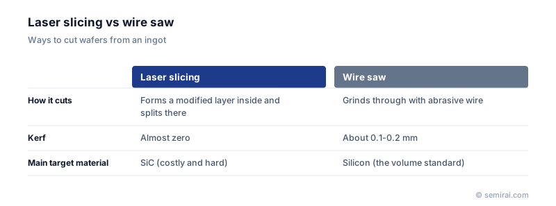
Laser slicing produces wafers by focusing a laser at a set depth inside an ingot to form a weakened, modified layer, then splitting a thin slice off along that layer. Because no material is sawn away, kerf loss is close to zero. It is of most interest for SiC, which is hard to saw and expensive to lose.
Also called: laser slicing, laser lift-off, LLO
Diagram
How it works
A laser wavelength that the material transmits is focused inside the crystal through an objective lens. Only near the focus is the intensity high enough for multiphoton absorption, so the material is modified locally while the surface is untouched. Scanning the focus across the ingot builds a plane of modified material. Thermal or mechanical stress then separates the crystal along that plane.
The principle is the same as stealth dicing, which separates finished wafers into chips along internal laser-modified lines; laser slicing applies it to cutting wafers from an ingot.
Benefits and challenges for SiC
SiC is so hard that wire sawing is slow, and kerf plus grinding and polishing allowance remove a large share of each expensive ingot. Laser slicing can increase the number of wafers per ingot considerably, which is why several companies are developing it.
The separated surface still carries residue of the modified layer and some roughness, which must be ground and polished away; if that allowance is large, much of the kerf saving is lost. Forming the layer requires scanning the whole area, so processing time per wafer becomes a throughput limit at larger diameters.
Laser lift-off
A related technique, laser lift-off (LLO), is used for GaN LEDs grown on sapphire. A laser shone through the sapphire decomposes the GaN at the interface, freeing the device layer from the growth substrate.
Japanese companies involved
- DISCO developed KABRA, a laser slicing process for SiC ingots, and supplies the equipment to run it.
- Hamamatsu Photonics developed the stealth dicing technology based on internal laser modification, the same principle that laser slicing uses.
- DISCO · Dicing, grinding and polishing equipment
- Tokyo Seimitsu (ACCRETECH) · Wafer probers, dicing and grinding machines, metrology
- Hamamatsu Photonics · Failure analysis, process monitoring and static elimination equipment
FAQ
Why does the laser not damage the surface?
The wavelength is chosen so the material is transparent to it at normal intensity. Absorption happens only where the beam is tightly focused and the intensity is very high, so energy is deposited inside the crystal at the focal depth.
Is laser slicing used for silicon wafers?
Silicon wafers are still sliced mainly with diamond wire saws, which are cheap and well established for silicon. The case for laser slicing is strongest where the material is hard and expensive, as with SiC.
Related pages
- Kerf Loss
- Wire Saw
- SiC Wafer (Silicon Carbide Substrate)
- Stealth Dicing
- Sapphire Substrate
- Wafer Thinning
- Wire saws and wafer slicing equipment
- Compound semiconductor substrate equipment (SiC/GaN)
- Tokyo Seimitsu (ACCRETECH) C-RW Series
- Asahi Diamond Industrial ECOMEP diamond wire
- Daiichi Kiden Solution Growth System
- Fujikoshi Machinery LSL-19A
Sources
Last updated: November 13, 2026