Nanotopography
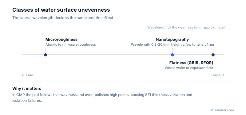
Nanotopography is shallow, gentle waviness of a wafer surface, with lateral wavelengths of about 0.2-20 mm and heights of a few to several tens of nanometres. It sits between flatness, which covers variation over tens of millimetres, and surface roughness, which covers features below a micrometre.
Also called: nanotopology, NT
Diagram
Why CMP made it important
Chemical mechanical polishing (CMP) presses the wafer against a polishing pad. The pad is compliant enough to follow gentle waviness, so the high points of the wave are polished faster and the film there becomes thinner. In shallow trench isolation (STI), this appears as uneven oxide thickness and over-polishing, which can lead to isolation failures.
Nanotopography mostly comes from the polishing steps of wafer manufacturing. Carrier thickness variation and pad condition in double-side polishing, or the way the wafer is held during final polishing, can leave periodic or near-periodic waves. Meeting flatness specifications is not enough; wafer makers must also suppress this intermediate band.
How it is measured
The surface shape is measured by interferometry or capacitive sensing, and a filter keeps only the target band of spatial wavelengths. A window of fixed size, for example 2 mm or 10 mm in diameter, is scanned across the surface, and the maximum peak-to-valley height inside the window is reported. Threshold height analysis (THA), which reports the share of the area above a height threshold, is also used.
Chipmakers include nanotopography in incoming wafer specifications and correlate it with CMP yield to manage quality differences between suppliers. Flatness, nanotopography, warp and roughness each describe a different spatial scale, and no single one describes surface quality on its own.
Japanese companies involved
- SUMCO and Shin-Etsu Chemical control nanotopography in their polishing processes for wafers used in CMP-intensive logic and memory production.
- Kobelco Research Institute makes wafer shape and flatness measurement systems of the kind used to evaluate nanotopography.
- Kobelco Research Institute · Wafer metrology: flatness and carrier lifetime
- SUMCO · Silicon wafers
- Shin-Etsu Chemical · Silicon wafers, photoresists and photomask blanks
FAQ
Is nanotopography the same as roughness?
No. Roughness covers very short wavelengths, from atomic scale up to micrometres, and affects things like gate oxide quality and light scattering. Nanotopography concerns millimetre-scale waves, too gentle to see as roughness but large enough to affect CMP.
Why is a filter needed?
A raw surface map mixes all wavelengths, including wafer-scale shape. Filtering removes the long-wavelength shape and the short-wavelength noise, so that the remaining signal reflects only the band that CMP is sensitive to.
Related pages
- Wafer Flatness (TTV / SFQR / GBIR)
- CMP (Chemical Mechanical Polishing)
- Dishing (CMP)
- Shallow Trench Isolation (STI)
- Silicon Wafer Manufacturing
- Dimple
- Microroughness
- Focus Leveling
- Wafer polishing and edge grinding equipment
- DISCO DFP8141
- Fujikoshi Machinery MCP-200
- Fujikoshi Machinery SPM-23
- Komatsu NTC GCG300
Sources
Last updated: November 13, 2026