Seed Crystal
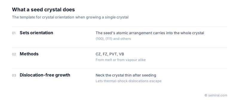
A seed crystal is a small piece of single crystal used as a template when growing a large single crystal. As atoms from the melt or vapour attach to it, they follow its lattice, so the orientation of the seed sets the orientation of the whole grown crystal. Seeds are used in the CZ, float zone and PVT methods.
Also called: seed, crystal seed
Diagram
Seeds in silicon growth
For Czochralski silicon, a rod-shaped seed cut along a chosen direction such as <100> or <111> is dipped just into the melt surface, and rotation and pulling begin. Most device wafers use the (100) surface because the Si/SiO₂ interface on that plane has a low density of interface states, which helps control the threshold voltage of MOS transistors. (111) is used for some power and bipolar devices.
The moment the seed touches the melt, thermal shock creates many dislocations. Necking, often called the Dash method, deals with this: the crystal is pulled very thin, a few millimetres in diameter, so the dislocations run out to the surface and disappear. Only then is the diameter increased to grow a dislocation-free crystal.
Seeds in SiC growth
In PVT growth of SiC, the source material is sublimated above 2,000 °C and the vapour recrystallises on a slightly cooler seed. The seed stays at high temperature for the whole run, and the new crystal inherits its defects, such as micropipes and dislocations. How the seed is mounted on its holder also matters, because poor attachment creates defects on the back side.
Seeds are cut from earlier high-quality crystals, so crystal quality is passed from one generation to the next. Improvements made in the past continue to benefit production quality, which is one reason accumulated know-how counts in crystal growth.
Japanese companies involved
- Shin-Etsu Chemical and SUMCO prepare and use seed crystals in growing CZ silicon ingots for their wafers.
- Shin-Etsu Chemical · Silicon wafers, photoresists and photomask blanks
- SUMCO · Silicon wafers
FAQ
Why is necking needed if the seed is already a perfect crystal?
Because the temperature difference between the seed and the melt creates new dislocations when they touch. Necking removes these before the crystal widens; without it the whole ingot would contain dislocations.
Do other materials use seed crystals too?
Yes. Compound semiconductors such as GaAs and InP are grown on seeds by vertical Bridgman (VB) and related methods, and sapphire and other oxide crystals are also seeded. In each case the seed sets the orientation.
Related pages
- Czochralski Process (CZ Method)
- Float Zone Process (FZ Method)
- PVT (Physical Vapour Transport) Method
- Silicon Ingot
- Crystal Plane Orientation
- Miller Index
- Single Crystal
- Vertical Bridgman Method (VB)
- Crystal growth furnaces
- Daiichi Kiden Round-Chamber Crystal Puller (CZ Method)
- Daiichi Kiden S278 / S380
- Ferrotec FT-CZ1200SE/1400SE
Sources
Last updated: November 13, 2026