Silicon (Si)
Silicon is the chemical element with atomic number 14 and symbol Si, and the base material of most semiconductor devices. It is abundant in the Earth's crust, has a bandgap of about 1.12 eV that is easy to control with dopants, and forms a high-quality insulating oxide by thermal oxidation. It should not be confused with silicone, a silicon-containing polymer.
Also called: Si, element 14
Diagram
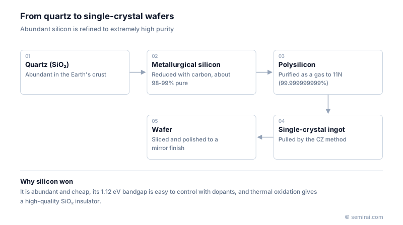
Why silicon became the main semiconductor
Silicon is the second most abundant element in the Earth's crust after oxygen, making up over a quarter of its mass, mostly as silicon dioxide (SiO₂) in quartz and sand. Its crystal has the diamond structure with a lattice constant of about 0.543 nm. The 1.12 eV bandgap is wide enough to keep leakage low at room temperature, and adding boron or phosphorus sets the conductivity type and level precisely.
The decisive advantage is its oxide. Heating silicon in oxygen grows a uniform SiO₂ film whose interface with the silicon has very few defects. This made the MOS transistor practical and supported decades of scaling. Silicon is also mechanically strong enough to handle as large wafers, and processes to grow nearly perfect 300 mm single crystals are well established. It melts at about 1,414 °C and has a density of about 2.33 g/cm³.
From quartz to wafers
Silicon is purified in several stages. Quartz is reduced with carbon in an electric arc furnace to make metallurgical-grade silicon of about 98 to 99 percent purity. This is reacted with hydrogen chloride to form trichlorosilane, which is purified by distillation and then decomposed onto heated silicon rods in the Siemens process, giving polycrystalline silicon of around eleven nines (99.999999999 percent) purity.
The polysilicon is melted and grown into single-crystal ingots, mainly by the Czochralski method, then sliced, ground and polished into wafers. Where silicon reaches its limits, in high-voltage power, high-frequency and light-emitting devices, compound semiconductors such as SiC, GaN and GaAs take over.
Japanese companies involved
- Shin-Etsu Chemical's wafer business and SUMCO are among the largest makers of silicon wafers.
- Tokuyama produces high-purity polycrystalline silicon for semiconductor use.
- Shin-Etsu Chemical · Silicon wafers, photoresists and photomask blanks
- SUMCO · Silicon wafers
- Tokuyama · Polysilicon and electronic chemicals
FAQ
What is the difference between silicon and silicone?
Silicon is the element, a hard grey solid used for chips and solar cells. Silicone is a family of polymers with a backbone of silicon and oxygen atoms carrying organic groups, used for sealants, rubbers and oils. Silicones are used in electronics, for example as encapsulants, but they are not semiconductors.
Is solar-grade silicon the same as semiconductor-grade silicon?
Both are made by similar routes, but semiconductor-grade polysilicon is purified much further, to around eleven nines, and has far tighter limits on metals, boron and phosphorus. Solar cells tolerate more impurities, so solar-grade material is cheaper.
Comparisons
Related pages
Sources
Last updated: November 2, 2026