Nano-Imprint Lithography (NIL)
Nano-imprint lithography (NIL) is a patterning technique that transfers a pattern by physically pressing a template, or stamp, engraved with nanoscale features into a liquid resin and then curing it. Because no light is projected through optics, resolution is not set by diffraction but by how finely the template itself can be made.
Also called: NIL, nanoimprint, UV nanoimprint lithography
Diagram
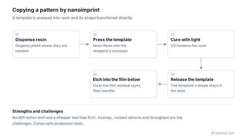
How the process works
In the jet-and-flash approach used for semiconductors, droplets of UV-curable resist are dispensed onto the wafer only where needed, matching the pattern density. A quartz template is lowered into the droplets, the liquid fills the template's recesses by capillary action, UV light cures it through the transparent template, and the template is lifted away.
A thin residual layer remains under the pattern, so a short etch clears it before the pattern is transferred into the underlying film. Templates are typically made from a master written by electron beam and then replicated, so a single master can supply many working templates.
Strengths and challenges
NIL can print very fine features with a simple, compact tool and low power use compared with EUV scanners. It suits repetitive, dense patterns such as memory arrays, and is also used for optical components and hard-disk media.
The challenges come from physical contact. Particles can damage the template or cause repeated defects, templates wear and must be inspected and replaced, overlay to existing layers must be controlled while the template touches the wafer, and throughput is limited by fill and cure time. These factors have kept NIL a complement to optical lithography rather than a replacement.
Japanese companies involved
- Canon develops and sells nanoimprint lithography systems for semiconductor manufacturing.
- Kioxia has worked on applying nanoimprint lithography to NAND flash production as a way to reduce lithography cost.
FAQ
How does NIL compare with EUV?
EUV projects any pattern through optics and is suited to complex logic layouts. NIL copies the template exactly, avoiding optics, and is best for repetitive patterns. NIL tools are simpler and use less energy, but defect control and overlay are harder.
What limits NIL resolution?
The template. Whatever can be written on the master by electron beam and faithfully replicated can be imprinted, along with the ability of the resist to fill and release from very small features.
Where else is nanoimprint used?
In optics and photonics, such as diffractive elements, wire-grid polarisers and waveguides for augmented-reality displays, as well as bit-patterned research on magnetic storage media.
Related pages
Sources
Last updated: November 2, 2026