Photoresist
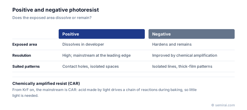
Photoresist is a light-sensitive material whose solubility in a developer changes where it is exposed, used in lithography to transfer circuit patterns onto a wafer. In positive resists the exposed areas dissolve; in negative resists they remain. Different chemistries are used for each exposure wavelength, from novolak resists to chemically amplified and metal-oxide resists for EUV.
Also called: resist, photo resist
Diagram
How a resist is used
The resist is spin-coated onto the wafer as a film tens to hundreds of nanometres thick and baked. The exposure tool projects the mask pattern into the film, a post-exposure bake drives the chemical reaction, and a developer, usually an aqueous alkaline solution, removes the soluble areas. The remaining resist pattern then protects the material underneath during etching or ion implantation and is stripped afterwards.
Resist processing is done on a coater/developer track linked to the exposure tool, so the bake temperatures and times are controlled as tightly as the exposure itself.
Resist chemistry by wavelength
For g-line and i-line exposure, resists combine a novolak resin with a diazonaphthoquinone (DNQ) photoactive compound. From KrF onwards, chemically amplified resists (CARs) became standard: light generates an acid, and during the post-exposure bake each acid molecule catalyses many deprotection reactions, so a small dose produces a large change in solubility. KrF resists are based on polyhydroxystyrene, while ArF resists use acrylic polymers that are transparent at 193 nm.
EUV resists face a three-way trade-off between resolution, line edge roughness and sensitivity. EUV photons are few and energetic, so random variation in how many photons arrive causes roughness and stochastic defects. Metal-oxide resists, which absorb EUV more strongly, are being developed alongside improved chemically amplified resists.
Japanese companies involved
- JSR, Tokyo Ohka Kogyo (TOK), Shin-Etsu Chemical, Sumitomo Chemical and Fujifilm all supply photoresists for KrF, ArF and EUV lithography, making Japan the main source of advanced resists.
- JSR acquired Inpria, a US developer of metal-oxide EUV resists.
- JSR · Photoresists and semiconductor materials
- Tokyo Ohka Kogyo (TOK) · Photoresists and high-purity process chemicals
- Shin-Etsu Chemical · Silicon wafers, photoresists and photomask blanks
- Sumitomo Chemical · Photoresists and semiconductor process chemicals
- Fujifilm (semiconductor materials) · Photoresists, CMP slurries and process chemicals
FAQ
Which is more common, positive or negative resist?
Positive chemically amplified resists developed in alkaline developer have been the mainstream in front-end lithography. Negative-tone processes are used where they image a feature better, for example negative-tone development of ArF resists in an organic solvent to print small trenches and contact holes.
What is a chemically amplified resist?
A resist in which exposure creates a photoacid, and that acid then catalyses many reactions during baking. The amplification makes the resist far more sensitive, which mattered when KrF lasers delivered much less usable light than mercury lamps. The trade-off is acid diffusion, which blurs the image slightly.
Why does each wavelength need its own resist?
The polymer must be transparent enough at the exposure wavelength for light to reach the bottom of the film, and must absorb efficiently enough to react. Polymers that work at 248 nm absorb too strongly at 193 nm, and EUV resists need elements that absorb 13.5 nm light well.
Related pages
Sources
Last updated: November 2, 2026