Notching
Notching is a dry etching defect in which the base of a pattern is cut sideways, leaving a notch, where the film being etched sits on an insulating layer. It typically occurs when polysilicon gates are etched down to the gate oxide, or when the silicon layer of a silicon-on-insulator (SOI) wafer is etched down to the buried oxide.
Also called: notch, foot notching
Diagram
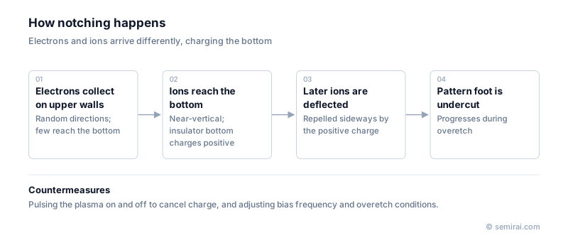
Why notching happens
The main cause is charging between features. Ions from the plasma arrive almost vertically and reach the bottom, while electrons arrive from random directions and tend to collect on the upper sidewalls of narrow trenches. The top of the trench charges negatively and the exposed insulator at the bottom charges positively.
Later ions are repelled by the positive charge at the bottom and deflected sideways into the foot of the pattern. Because the insulator cannot conduct the charge away, the effect is strongest once the underlying layer is exposed, during the overetch period.
Effects and countermeasures
A notch changes the gate length at the base of the gate, which spreads transistor characteristics, and narrows lines so that they break more easily. In deep silicon etching on SOI, it damages the bottom of MEMS structures.
Countermeasures include pulsing the plasma on and off so that charge at the bottom is neutralised during the off period, lowering the bias frequency to change ion behaviour, and changing overetch conditions. The term is unrelated to the notch cut into a wafer's edge to mark crystal orientation.
Japanese companies involved
- SAMCO makes ICP etch systems for deep silicon etching, including Bosch-process tools, where notching at the buried oxide of SOI wafers must be controlled.
- Tokyo Electron (TEL) and Hitachi High-Tech make etch systems used for gate etching, where notching at the gate oxide must be suppressed.
- SAMCO · Plasma etching, CVD and plasma cleaning equipment
- Tokyo Electron (TEL) · Coat/develop, etch and deposition equipment
- Hitachi High-Tech · CD-SEM metrology, defect inspection and etch systems
FAQ
Why does notching happen only on insulators?
If the layer below is a conductor, the charge brought by ions can spread out and escape, so little charge builds up. On an insulator the positive charge stays where it lands and deflects later ions. This is why gate etching on oxide and silicon etching on SOI buried oxide are typical cases.
Why does a pulsed plasma reduce notching?
When the plasma is switched off, electron temperature falls quickly and negative ions can form and reach the bottom of features. These negative particles cancel the positive charge that built up there, so ions in the next on period are not bent sideways as much.
Related pages
Sources
Last updated: November 13, 2026