Plasma Sheath
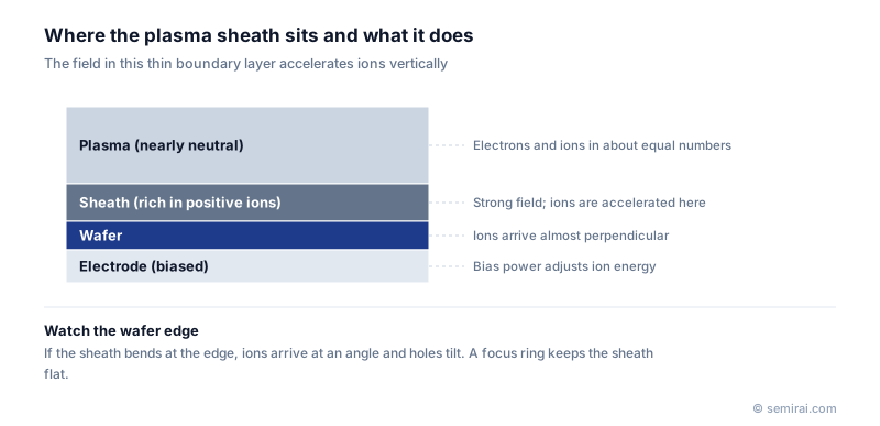
A plasma sheath is the thin layer, low in electrons and rich in positive ions, that forms where a plasma meets a wall, electrode or wafer. The body of the plasma is nearly neutral, but the sheath holds a strong electric field and a large potential drop toward the surface. This field is what lets plasma etching drive ions vertically into the wafer.
Also called: sheath, Debye sheath
Diagram
Why a sheath forms
Electrons are thousands of times lighter than ions and move far faster. When a plasma first touches a surface, electrons reach it more quickly and charge it negatively. That negative potential then repels electrons and attracts ions until the two currents balance, leaving a positive space-charge layer in front of the surface.
Ions entering the sheath are accelerated by its field and strike the surface almost perpendicularly. Sheath thickness depends on the voltage across it and on plasma density. It is a few Debye lengths at a floating wall but can reach the millimetre range on a wafer with a strong RF bias. Changing the bias power and frequency changes the sheath voltage, which controls the energy of ions reaching the wafer and how that energy is distributed.
How the sheath shapes etch profiles
At the wafer edge, the step to the surrounding parts and the change of material bend the sheath boundary. Ions then arrive at an angle and holes near the edge are etched with a tilt. A focus ring around the wafer extends the flat sheath beyond the wafer edge. As the ring is eroded its height changes and the sheath bends again, so rings are replaced or their height is adjusted.
Inside deep holes, the difference between vertically arriving ions and randomly directed electrons charges the bottom and sidewalls, which can distort the profile and cause notching. Understanding the sheath is basic to designing etch and plasma CVD conditions.
Japanese companies involved
- Tokyo Electron (TEL) designs etch chambers in which sheath control at the wafer edge, including the focus ring, is an important factor in edge uniformity.
- Tokyo Electron (TEL) · Coat/develop, etch and deposition equipment
FAQ
What is the Debye length?
It is the distance over which a plasma screens out a local electric charge. It grows with electron temperature and shrinks with plasma density, and is typically well under a millimetre in processing plasmas. Sheaths are several Debye lengths thick or more.
Why does the focus ring need replacing?
The ring is exposed to the same plasma as the wafer and is slowly etched away. As it gets thinner, the sheath above it drops and bends at the wafer edge, tilting the ions there. Replacing the ring, or raising it, restores a flat sheath and vertical etching at the edge.
Related pages
- Plasma (Semiconductor Processing)
- Self-bias (DC Self-bias)
- RIE (Reactive Ion Etching)
- ICP (Inductively Coupled Plasma)
- CCP (Capacitively Coupled Plasma)
- Charge-up
- Microloading Effect
- Aspect Ratio
- Dry etching equipment
- Tokyo Electron (TEL) Acrevia™
- Tokyo Electron (TEL) Tactras™
- Daihen RF generators and auto matching units (RGA/WGA/MGA/FGA series)
- Elionix EIS-200ERP
Sources
Last updated: November 13, 2026