Optical Emission Spectroscopy (OES)
Optical emission spectroscopy (OES) analyses the light a plasma emits, separated by wavelength with a spectrometer, to find which atoms and molecules are present and in what amounts. Species excited by electron collisions emit light at wavelengths characteristic of each species as they relax, so the spectrum reveals the composition of the plasma.
Also called: OES, plasma emission spectroscopy
Diagram
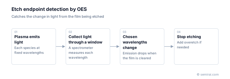
Endpoint detection
The most common use in semiconductor manufacturing is detecting the endpoint of dry etching. While an oxide film is being etched, for example, products released from the film, such as carbon monoxide, emit strongly. When the film is cleared and the layer below is exposed, that emission weakens and emission from other species grows. Watching this change tells the tool when to stop, or when to switch to a gentler overetch step.
The light is collected through a window in the chamber, so the method needs no contact with the wafer and works in real time.
Low open area and other uses
When only a small fraction of the wafer is being etched, the amount of material removed is small and the emission change is slight. Tools then analyse many wavelengths together with statistical methods to pick out the endpoint.
OES data are also used to follow chamber condition, such as deposit build-up on the walls and the progress of seasoning, to detect wear of parts and signs of abnormal discharge, and as input to virtual metrology, which estimates process results without measuring every wafer, and to predictive maintenance.
Japanese companies involved
- Hamamatsu Photonics makes spectrometers and photodetectors used to monitor plasma emission and detect etch endpoints.
- HORIBA makes process monitoring instruments for semiconductor equipment, including plasma emission monitors.
- Hamamatsu Photonics · Failure analysis, process monitoring and static elimination equipment
- HORIBA · Mass flow controllers and process monitoring instruments
- Tokyo Electron (TEL) · Coat/develop, etch and deposition equipment
FAQ
Why does OES show the etch endpoint?
Products formed from the film being etched emit light at fixed wavelengths. Once the film is gone, those products stop forming and the emission drops, while emission tied to the underlying layer may rise. Tracking a few chosen wavelengths gives a clear signal for when to stop.
Why is a small open area hard to detect?
If only a small percentage of the wafer surface is exposed to the etch, little material is removed and the emission change is tiny compared with noise and the background plasma light. Multivariate analysis across the whole spectrum is used to extract such small changes.
Related pages
Sources
Last updated: November 13, 2026