PVT (Physical Vapour Transport) Method
Physical vapour transport (PVT), also called the sublimation or modified Lely method, grows single crystals by sublimating a source material at high temperature and letting the vapour, driven by a temperature gradient, recrystallise on a seed crystal. It is used for materials such as SiC and AlN that cannot be pulled from a melt.
Also called: physical vapor transport, sublimation method, modified Lely method
Diagram
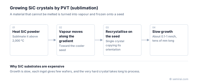
How SiC is grown by PVT
SiC powder sits at the bottom of a graphite crucible and a seed crystal is fixed at the top. The whole assembly is heated to roughly 2,000-2,500 °C under low pressure. The source is kept slightly hotter than the seed, so vapour species such as Si, Si₂C and SiC₂ rise along the gradient, become supersaturated at the seed and deposit as crystal.
Growth runs at roughly 0.1-1 mm per hour and a run takes days. A silicon CZ ingot can reach about two metres; a PVT SiC boule is only a few tens of millimetres long. The much smaller number of wafers per growth run is a main reason SiC substrates cost far more than silicon wafers.
Defects and what comes next
Micropipes, hollow cores that once killed devices, have been almost eliminated by improved growth conditions. Basal plane dislocations (BPDs) remain the main concern, because they can expand into stacking faults under current and raise on-resistance over time (bipolar degradation). Temperature and pressure must also be controlled to keep the crystal in the 4H polytype.
Faster methods such as top-seeded solution growth and high-temperature CVD are under study, but PVT remains the production standard. The move from 150 mm to 200 mm diameter is a key part of reducing SiC device cost.
Japanese companies involved
- Resonac and Sumitomo Electric Industries are Japanese producers of SiC wafers for power devices, and both work on SiC crystal and epitaxial wafer technology.
- Resonac · CMP slurries, packaging materials and SiC epitaxial wafers
- Sumitomo Electric Industries (compound semiconductors) · SiC epitaxial wafers and GaAs and InP substrates
FAQ
Why can't SiC be grown by the Czochralski method?
At normal pressure SiC does not melt; it decomposes and sublimates when heated. There is no melt to pull from, so the crystal has to be built up from the vapour phase instead.
How are basal plane dislocations reduced?
They cannot be removed completely in the substrate. During epitaxial growth, conditions are chosen so that most BPDs reaching the surface convert into threading edge dislocations, which do not cause bipolar degradation.
Related pages
- SiC Wafer (Silicon Carbide Substrate)
- Seed Crystal
- Silicon Carbide (SiC)
- Czochralski Process (CZ Method)
- Epitaxial Wafer (Epi Wafer)
- GaN-on-Silicon (GaN-on-Si)
- Wide Bandgap Semiconductor (WBG)
- Dislocation
- Compound semiconductor substrate equipment (SiC/GaN)
- Crystal growth furnaces
- Daiichi Kiden Round-Chamber Crystal Puller (CZ Method)
- Daiichi Kiden S278 / S380
- Daiichi Kiden Solution Growth System
- Ferrotec FT-CZ1200SE/1400SE
Sources
Last updated: November 13, 2026