Planarisation (Planarization)
Planarisation is the collective term for processes that remove the steps that form on the wafer surface during manufacturing and make it flat. When transistors and wiring are stacked in many layers, each pattern is copied into the surface above, and the topography grows with every level. Flattening each layer is a precondition for building fine devices.
Also called: planarization, surface planarisation, global planarisation
Diagram
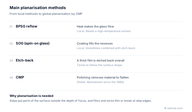
Why flatness is needed
The first reason is lithography depth of focus. If the surface has steps, some areas fall outside the focus range and the pattern blurs. The second is film deposition and etching: films and wires become thin or break at step edges, and etching leaves residues along them.
There are two levels of flatness. Local planarisation smooths steps over a short distance near a pattern. Global planarisation evens out the height across a whole chip or wafer, including the difference between dense and sparse pattern areas.
Methods over time
Early methods included reflow of borophosphosilicate glass (BPSG), which flows when heated; spin-on glass (SOG), which fills recesses as it is coated; and etch-back, in which a thick film is etched back uniformly. These mainly gave local planarisation.
From the 1990s, chemical mechanical polishing (CMP) became the main method because it can planarise globally. It is now used at many levels, from transistor isolation to wiring. To limit CMP variation, designers add dummy patterns in empty areas so that pattern density is more uniform.
Japanese companies involved
- Ebara builds CMP systems, the main planarisation tools in today's fabs.
- Resonac and Fujimi Incorporated supply the slurries used in CMP planarisation.
- Ebara · CMP systems, dry vacuum pumps and exhaust treatment
- Resonac · CMP slurries, packaging materials and SiC epitaxial wafers
- Fujimi Incorporated · CMP slurries and polishing materials
FAQ
What is the difference between local and global planarisation?
Local planarisation smooths steps over a short range around a feature. Global planarisation makes the height uniform across the chip or wafer, removing differences between areas of different pattern density. Reflow and SOG are mainly local; CMP achieves global flatness.
Are planarisation and CMP the same thing?
No. Planarisation is the goal, and CMP is one way to reach it. Because CMP now does most planarisation work the terms are often used loosely, but reflow, etch-back and spin-on films are also planarisation methods.
Related pages
Sources
Last updated: November 1, 2026