Polishing Pad (CMP Pad)
A polishing pad is the consumable mounted on the rotating platen of a CMP tool. It holds and transports slurry and presses it against the wafer, so it acts both as a slurry carrier and as the elastic body that transmits pressure. Most pads are made of porous polyurethane, and their hardness, pores and grooves strongly shape the result of polishing.
Also called: CMP pad, polishing cloth
Diagram
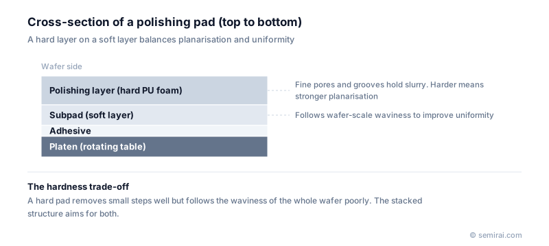
Structure of a pad
The standard pad for device CMP is a hard polyurethane layer containing closed micro-pores tens of micrometres across. When the surface is cut open, the pores become small pockets that hold slurry. The surface also has grooves, typically concentric circles or an X-Y grid, which distribute fresh slurry under the wafer and carry away polishing debris. Groove shape and pitch change how long slurry stays under the wafer and therefore affect removal rate and uniformity.
For final polishing, such as the last step on bare silicon wafers, softer suede-type pads with a napped surface are used because they leave a smoother, less damaged surface.
Hardness: planarisation versus uniformity
A hard pad does not bend into small recesses, so it presses mainly on raised features and removes them first. This gives strong planarisation over short distances. The same stiffness, however, prevents the pad from following the gentle bow and thickness variation of the whole wafer, so within-wafer uniformity suffers. A soft pad behaves the other way round.
Most pads therefore stack a hard polishing layer on a softer subpad, bonded to the platen with adhesive. The hard top layer flattens local topography while the subpad lets the pad follow wafer-scale shape.
Glazing, conditioning and pad life
During use the surface asperities are flattened and pores fill with debris, an effect called glazing. The pad then holds less slurry and the removal rate falls. A diamond disk conditioner sweeps across the pad, usually during polishing, to cut a fresh rough surface. Because the pad slowly wears, removal rate drifts over its life, and fabs combine endpoint detection and run-to-run control to keep film thickness on target. Replacing a pad stops the tool and the new pad needs a break-in period before it polishes steadily.
Japanese companies involved
- Nitta DuPont, a joint venture of Nitta and DuPont, makes CMP pads and wafer polishing pads in Japan.
- Fujibo makes polishing pads for CMP and for silicon wafer polishing, including suede-type pads used in final polishing.
- Ebara builds CMP systems, the tools on which these pads are mounted.
- Ebara · CMP systems, dry vacuum pumps and exhaust treatment
- Nitta DuPont · CMP and wafer polishing pads
- Fujibo · Polishing pads for CMP and wafer polishing
FAQ
Why does a polishing pad need grooves?
Without grooves the wafer would hydroplane on a film of slurry, and fresh slurry would struggle to reach the centre of the wafer. Grooves channel slurry in, let used slurry and debris escape, and reduce suction between pad and wafer.
What does pad conditioning do?
A disk embedded with diamond particles abrades the pad surface, removing glazed material and reopening pores. Conditioning keeps removal rate stable, but it also consumes the pad, so conditioner force and sweep are balanced against pad life.
Are pads the same for every CMP step?
No. Oxide, STI, copper, barrier and tungsten steps often use different pad hardness, porosity and groove patterns, and multi-platen tools may use a hard pad for bulk removal and a softer pad for the final buff.
Related pages
Sources
Last updated: November 12, 2026