Focus Leveling
Focus leveling is the function by which an exposure tool measures the height and tilt of the wafer surface and adjusts the wafer stage so that the area being exposed stays within the projection lens's depth of focus. It is like automatic focusing on a camera, performed for every exposure field.
Also called: focus and leveling, autofocus, level sensor
Diagram
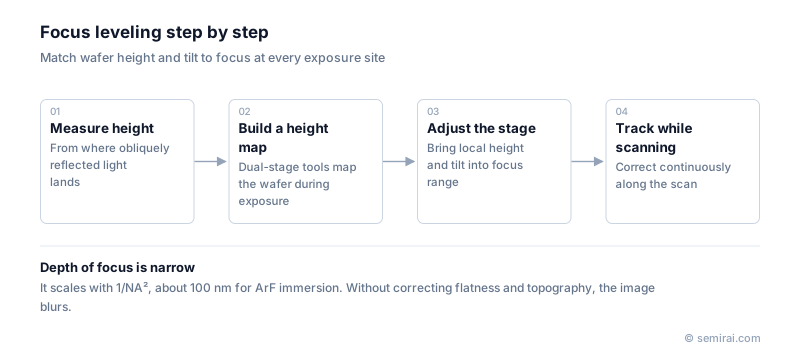
Why focus control has become so tight
Depth of focus, the height range over which the image stays sharp, shrinks as features shrink. It scales with wavelength and inversely with the square of the numerical aperture (NA), so in ArF immersion lithography it is on the order of 100 nm, and narrower still in high-NA EUV.
The wafer surface is not perfectly flat. The substrate itself varies in flatness, and earlier process steps leave topography. Unless these height differences are measured and corrected just before exposure, parts of the field fall out of focus and the pattern blurs.
How height is measured
A common method is a level sensor that shines light onto the wafer at a shallow angle and calculates height from the shift in position of the reflected beam. In a scanner, height and tilt are followed continuously along the scan direction while the field is exposed.
Tools with two wafer stages measure a height map of the whole wafer on one stage while the other stage is exposing, which keeps accuracy high without lowering throughput. The wafer edge remains difficult, because the surface shape changes abruptly there.
Japanese companies involved
- Nikon and Canon build lithography steppers and scanners that incorporate their own focus and leveling systems.
FAQ
What is depth of focus?
It is the allowable range of wafer height within which the projected image stays sharp enough to print. By the Rayleigh relation it is proportional to wavelength and inversely proportional to NA squared, so raising NA to improve resolution narrows the focus margin, which is why leveling became critical.
Why is focus hard at the wafer edge?
The outer few millimetres of a wafer roll off or tilt because of polishing and deposition, so height changes sharply within one exposure field. Part of the level sensor's measurement spot may also fall off the wafer. These effects make edge dies more prone to defocus and lower yield.
Related pages
Sources
Last updated: November 1, 2026