Tungsten (W)
Tungsten is the metal with atomic number 74 and symbol W, which comes from its German name Wolfram. It has the highest melting point of all metals, about 3,422 °C, and a density of about 19.3 g/cm³. In chips it fills the contacts that connect transistors to the wiring above and forms word lines in DRAM and 3D NAND.
Also called: W, wolfram
Diagram
Contact plugs
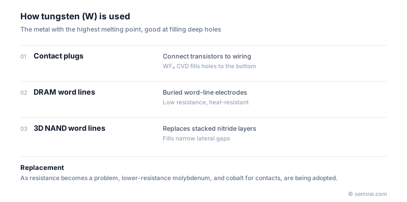
The largest use of tungsten is in contact plugs. Narrow, deep holes connecting the transistor's source, drain and gate to the first copper wiring level are filled by CVD, in which tungsten hexafluoride (WF₆) is reduced with hydrogen or silane. Tungsten CVD fills holes to the bottom without voids, tolerates later high-temperature steps and, unlike copper, does not diffuse into silicon and contaminate devices. That makes it well suited to the level closest to the transistor.
Before filling, a titanium and titanium nitride liner is deposited on the hole walls. It gives adhesion and protects the underlying layers from the fluorine in WF₆. After filling, excess tungsten on the surface is removed by CMP (chemical mechanical polishing).
Memory word lines and replacement
Tungsten forms the buried word lines of DRAM and the word-line electrodes of 3D NAND. In 3D NAND, stacked sacrificial nitride layers are removed and the resulting horizontal gaps are filled with tungsten, so tungsten use grows as layer counts rise.
As lines and contacts shrink, tungsten's resistance and the space taken by its liner become a problem. Molybdenum, which can give lower resistance in very narrow features and may not need a liner, is being introduced for some word lines and contacts, and cobalt has been used for contacts in some logic processes. Tungsten ore production is heavily concentrated in China, so tungsten is treated as a critical mineral.
Japanese companies involved
- A.L.M.T. (Allied Material), a Sumitomo Electric group company, makes tungsten and molybdenum products, including materials for semiconductor applications.
- Tokyo Electron (TEL) · Coat/develop, etch and deposition equipment
FAQ
Why is copper not used for contacts as well?
Copper diffuses quickly into silicon and degrades transistors, and it would need a thick barrier in a very small hole. Tungsten does not diffuse into silicon, fills narrow holes conformally and survives high temperatures, so it remains at the contact level while copper is used for the wiring above.
Why does tungsten resistance rise in small features?
In very thin lines, electrons scatter at surfaces and grain boundaries, raising resistivity above the bulk value. The Ti/TiN liner also takes up a larger share of the cross-section as features shrink, leaving less room for the conductor itself.
Related pages
Sources
Last updated: November 2, 2026