Temporary Bonding and Debonding (TBDB)
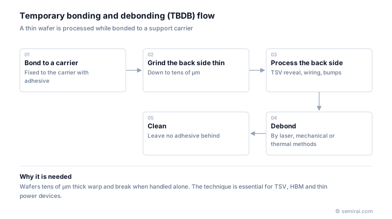
Temporary bonding and debonding (TBDB) is a technique in which a processed device wafer is glued temporarily to a support carrier of glass or silicon, thinned and processed on the back, and then released from the carrier. It is used wherever wafers are thinned to a few tens of micrometres, as in TSV-based 3D stacking, HBM and thin power semiconductors.
Also called: temporary bonding, debonding, TBDB
Diagram
Why a carrier is needed
Below roughly 50 µm, a wafer bows under its own weight and film stress and breaks easily, so it can no longer be transported or processed alone. The wafer is therefore bonded face-down to a carrier with a temporary adhesive, giving a stack that behaves like a normal-thickness wafer.
With the carrier attached, the back side is ground (backgrinding), polished by CMP, etched to reveal the TSVs, and given back-side wiring and bumps. Afterwards the thin wafer is transferred onto dicing tape and the carrier is removed.
What the adhesive must do
The temporary adhesive faces conflicting demands. It must survive process heat of roughly 200-300°C, chemicals and vacuum without releasing, yet come away cleanly at the end without damaging the devices. Its thickness must also be very uniform, because grinding takes the carrier surface as its reference. After debonding, residue is removed with solvents or plasma.
Debonding methods
There are four main methods. Thermal slide heats the adhesive until it softens and slides the wafer off sideways. Mechanical debonding peels the wafer from one edge. Laser debonding shines a laser through a glass carrier to decompose a release layer. Solvent debonding dissolves the adhesive. Laser and mechanical methods put less force on the wafer and are fast, and are now widely used. TBDB should not be confused with permanent wafer bonding or hybrid bonding, which join wafers for good as part of the device.
Japanese companies involved
- Tokyo Electron supplies wafer bonding and debonding equipment, and DISCO makes the grinders and polishers used to thin bonded wafers.
- Tokyo Electron (TEL) · Coat/develop, etch and deposition equipment
- DISCO · Dicing, grinding and polishing equipment
FAQ
Why use a glass carrier rather than silicon?
Glass is transparent, so laser or UV light can pass through it to release the adhesive layer, and its thermal expansion can be tuned to match silicon. Silicon carriers suit processes that cannot tolerate glass or that use thermal or mechanical release.
What can go wrong during debonding?
The thin wafer can crack or chip at the edge if too much force is applied, and adhesive residue can remain on bumps. Debonding is therefore done with the wafer supported on tape and a frame, followed by careful cleaning and inspection.
Related pages
Sources
Last updated: November 13, 2026