GaN-on-Silicon (GaN-on-Si)
GaN-on-Si is a substrate technology in which gallium nitride (GaN) layers are grown heteroepitaxially on inexpensive, large-diameter silicon wafers. It avoids the high cost of free-standing GaN or SiC substrates and lets GaN devices be processed with the equipment and wafer sizes (150 mm and 200 mm) of existing silicon lines.
Also called: GaN on Si, gallium nitride on silicon
Diagram
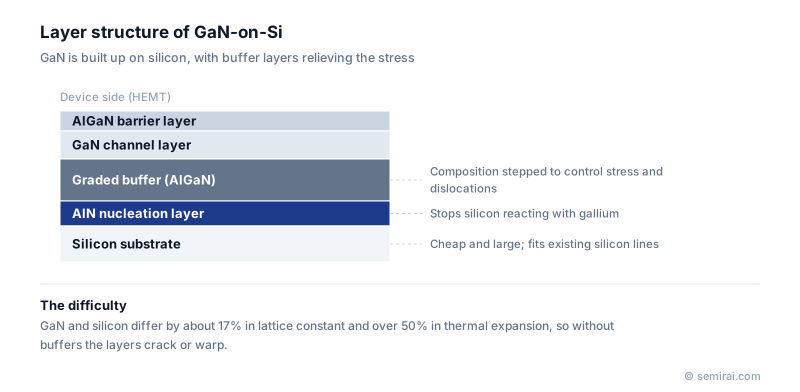
Why growing GaN on silicon is hard
GaN and silicon are poorly matched. Their lattice constants differ by about 17%, and their thermal expansion coefficients differ by more than 50%. GaN grown directly on silicon would contain a very high density of dislocations and would crack under tensile stress as the wafer cools from growth temperature.
To manage this, growers use a multilayer stack: an aluminium nitride (AlN) nucleation layer, then buffer layers whose aluminium content is stepped or graded, or superlattice buffers. These layers control stress and bend or annihilate dislocations before the device layers are grown on top.
A second problem is meltback etching. At high temperature, gallium reacts with silicon and can eat deeply into any exposed silicon surface. The silicon must therefore be completely covered with AlN, which does not react with it, before any gallium-containing layer is grown. The layers are grown by metal-organic chemical vapour deposition (MOCVD); AIXTRON and Veeco are major suppliers of these reactors.
Where GaN-on-Si is used
The main application is the GaN high-electron-mobility transistor (HEMT) used as a fast, efficient power switch. In the voltage range up to about 650 V, such as fast chargers and data-centre power supplies, GaN-on-Si HEMTs are replacing silicon MOSFETs. RF front-end parts and micro-LEDs are further applications.
Japanese companies involved
- Sumitomo Electric Industries makes GaN HEMTs on SiC substrates for radio-frequency applications, the high-power alternative to GaN-on-Si.
- Sumitomo Electric Industries (compound semiconductors) · SiC epitaxial wafers and GaAs and InP substrates
FAQ
How does GaN-on-Si compare with GaN-on-SiC?
SiC conducts heat much better, so GaN-on-SiC is still preferred for high-power RF amplifiers. Silicon wins on cost and wafer diameter, which makes GaN-on-Si the usual choice for power switches up to about 650 V and for consumer products.
Why does GaN-on-Si need such a thick buffer?
The buffer has to absorb the stress from the thermal expansion mismatch so the wafer does not crack or warp too much when it cools. It must also be highly insulating so that it can hold off the device voltage between the channel and the conductive silicon substrate.
Can the silicon substrate be removed?
Yes. Some research and products remove the silicon after growth and transfer only the device layers to another carrier, for example to improve heat removal. The choice of substrate is a trade-off between cost, heat dissipation and wafer size.
Related pages
- Gallium Nitride (GaN)
- High Electron Mobility Transistor (HEMT)
- Epitaxy (Epitaxial Growth)
- Sapphire Substrate
- Wide Bandgap Semiconductor (WBG)
- Power Semiconductor
- Dislocation
- Lattice Constant
- Compound semiconductor substrate equipment (SiC/GaN)
- Compound semiconductor equipment
- Power semiconductor manufacturing equipment
- Advantest EXAVIS
- Advantest MT100 / MT200
- Canon ANELVA EC8100
- Daiichi Kiden Solution Growth System
Sources
Last updated: November 13, 2026