Current Collapse
Current collapse is an effect in gallium nitride high electron mobility transistors (GaN HEMTs) in which, after the device has blocked a high voltage in the off state, it conducts less current than expected when turned on. Because the on-resistance changes with every switching cycle, it is also called dynamic on-resistance increase.
Also called: dynamic on-resistance, dynamic RDS(on)
Diagram
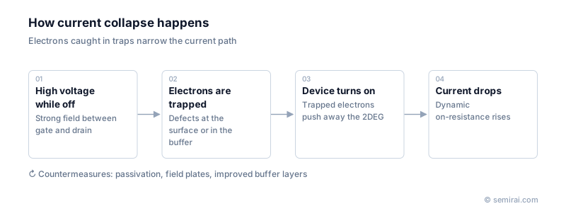
What causes current collapse
The main cause is electrons caught in traps, which are defects in the crystal or at its surface. While the device is off and blocking a high voltage, the strong field between gate and drain accelerates electrons, and some become trapped at the device surface or in the buffer layer beneath the GaN channel.
Trapped electrons act as fixed negative charge. They push away the two-dimensional electron gas that forms the current path, so when the device is turned on, the channel is partly depleted and the current is lower. Because electrons take time to escape from the traps, the effect persists for a while, from microseconds to much longer depending on the trap. The name comes from the way the current-voltage curves appear to collapse.
How it is suppressed
Several countermeasures are combined. The surface is covered with a passivation film, such as silicon nitride, to reduce surface traps. Field plates extending from the gate or source spread out the electric field at the gate edge, so fewer electrons are accelerated enough to be trapped. The buffer layer is optimised in crystal quality and in how dopants such as carbon, used to make it insulating, are introduced.
Current collapse was one of the major barriers to commercial GaN power devices. Today's products show much smaller effects, but dynamic on-resistance remains an important item in GaN reliability testing.
Japanese companies involved
- Sumitomo Electric Industries makes GaN HEMTs for wireless base stations and other radio-frequency uses, where trapping effects are also a design concern.
- ROHM and Renesas Electronics make GaN power devices and qualify them for dynamic on-resistance.
- ROHM · SiC and silicon power devices, analog ICs
- Sumitomo Electric Industries (compound semiconductors) · SiC epitaxial wafers and GaAs and InP substrates
- Renesas Electronics · Microcontrollers, automotive SoCs, analog and power chips
FAQ
Does current collapse still occur in commercial GaN devices?
It was a serious problem in early devices, but passivation, field plates and better buffers have reduced it greatly. A small effect can remain at high voltage or temperature, so manufacturers measure dynamic on-resistance under repeated high-voltage switching and reflect it in specifications.
Does a similar effect occur in SiC MOSFETs?
Current collapse is specific to GaN HEMTs. SiC MOSFETs have a different issue: traps at the gate oxide interface can shift the threshold voltage over time. The causes and countermeasures are not the same.
Related pages
Sources
Last updated: November 2, 2026