Passivation
Passivation means making a surface chemically and electrically inactive to protect it. In semiconductors it mainly refers to the protective film, typically silicon nitride with oxide and sometimes polyimide, that covers the top of a chip to shield wiring and devices from moisture, mobile ions and scratches.
Also called: passivation layer, surface passivation
Diagram
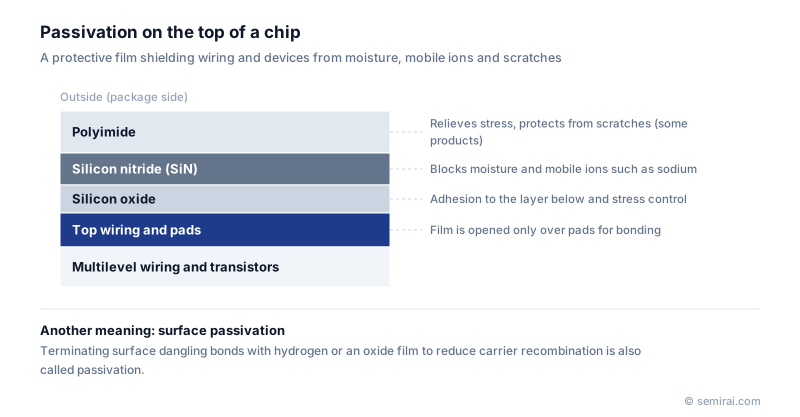
The chip passivation layer
Passivation is the last front-end step. Over the top metal layer, silicon nitride (SiN), often stacked with silicon oxide, is deposited by plasma-enhanced CVD. A polyimide layer may be added to relieve stress and improve adhesion to the mould compound. Silicon nitride is dense and blocks water and mobile ions such as sodium, which would otherwise corrode the wiring or shift transistor characteristics.
The film is then opened only over the bond pads so that wires or bumps can be attached. Cracks or pinholes in the passivation let moisture that has diffused through the package reach the wiring, so reliability is checked with tests such as highly accelerated stress testing (HAST) at high temperature and humidity.
Surface passivation
The term also covers treatments that tie up dangling bonds, atoms at a surface or interface missing a bonding partner, to reduce carrier recombination and charge trapping. In silicon devices, an anneal in hydrogen-containing forming gas terminates traps at the gate oxide interface.
In solar cells, aluminium oxide films and hydrogen-rich silicon nitride films passivate the surface and raise conversion efficiency considerably. In GaN high-electron-mobility transistors (HEMTs), a silicon nitride surface layer reduces current collapse, a drop in current caused by electrons trapped at the surface. In metallurgy, passivation also means forming a protective oxide on a metal to stop corrosion.
Japanese companies involved
- Samco makes plasma CVD systems that deposit silicon nitride and silicon oxide films, including passivation layers for compound semiconductor and power devices.
- Tokyo Electron and Kokusai Electric supply deposition equipment for nitride and oxide films used across the front-end process.
- SAMCO · Plasma etching, CVD and plasma cleaning equipment
- Tokyo Electron (TEL) · Coat/develop, etch and deposition equipment
- Kokusai Electric · Batch deposition, diffusion and ALD equipment
FAQ
Why is silicon nitride preferred for passivation?
Silicon nitride is dense, has low permeability to water and blocks mobile ions such as sodium far better than silicon oxide. It is also hard enough to resist scratches during handling and assembly, and plasma CVD can deposit it at temperatures the metal wiring tolerates.
Why is polyimide added on top?
Polyimide is a tough organic film that cushions the stress from the plastic mould compound and from temperature cycling, protects against filler particles in the package and improves adhesion. It is also used as a dielectric in redistribution layers.
Related pages
- PECVD (Plasma-Enhanced Chemical Vapour Deposition)
- Interlayer Dielectric (ILD)
- Multilevel Interconnect
- Epoxy Molding Compound (EMC)
- HAST (Highly Accelerated Stress Test)
- Solar Cell (Photovoltaic Cell)
- Carrier Recombination
- High Electron Mobility Transistor (HEMT)
- CVD equipment
- Kokusai Electric QUIXACE®
- Kokusai Electric QUIXACE®-II
- Kokusai Electric QUIXACE ULTIMATE®
- SAMCO PD-220NL
Sources
Last updated: November 13, 2026