Design for Testability (DFT)
Design for testability (DFT) is the set of design techniques that build test circuitry into a chip at the design stage so it can be tested efficiently after manufacturing. Its aims are high fault coverage, short test time and low test cost, and it is an essential part of every modern SoC design.
Also called: DFT, design for test
Diagram
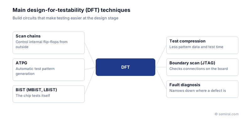
Main DFT techniques
Scan design is the foundation. The chip's flip-flops are linked into long shift registers, called scan chains, so that a tester can load any internal state, run one clock, and shift the result out. This turns a hard sequential-circuit problem into a manageable combinational one, which is what makes automatic test pattern generation (ATPG) practical.
Built-in self-test (BIST) puts pattern generators and result checkers on the chip itself. Memory BIST (MBIST) is used on almost every embedded memory, and logic BIST (LBIST) is common in automotive chips. Boundary scan, standardised as IEEE 1149.1 (JTAG), adds cells at the I/O pins so that connections can be checked after the chip is mounted on a board. Test compression reduces the data that has to be shipped through the scan pins.
Trade-offs and new challenges
Test logic takes area and power and can affect timing, so DFT engineers balance coverage against the chip's power, performance and area. Test points are added where faults are hard to control or observe, and diagnosis features help locate defects found in production.
Large SoCs contain many IP blocks, each with its own test structures. IEEE 1687 (IJTAG) defines a way to access and control these embedded instruments in a uniform manner. Chiplets add another layer: each die must be tested before assembly, and the links between dies in the package must be tested afterwards.
Japanese companies involved
- Advantest's automatic test equipment applies the scan, compression and BIST patterns that DFT flows produce, so DFT decisions directly affect how long each chip spends on a tester.
- Advantest · Automated test equipment (ATE) for SoC and memory
FAQ
Who provides DFT tools?
DFT insertion and ATPG are done with electronic design automation (EDA) tools. The main suppliers are Synopsys, Cadence and Siemens EDA, whose tools insert scan chains, compression and BIST and then generate and grade the test patterns.
Why not test chips only by running their functions?
Functional tests check that a design meets its specification but give no reliable measure of how many manufacturing defects they would catch, and writing them by hand for billions of transistors is impossible. DFT plus ATPG produces compact patterns with a measurable fault coverage.
Related pages
Sources
Last updated: November 2, 2026