ESD Test (HBM / CDM)
ESD testing measures a device's robustness against electrostatic discharge (ESD). Static charge built up on people, equipment or the device itself can flow into a pin in a fraction of a microsecond and rupture gate dielectrics or melt junctions, so devices are stressed under standardised discharge conditions to find the level they can withstand.
Also called: electrostatic discharge test, ESD robustness test, human body model, charged device model
Diagram
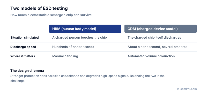
Human body model and charged device model
The human body model (HBM) simulates a charged person touching a pin. A 100 pF capacitor is discharged into the device through a 1.5 kΩ resistor, giving a pulse that lasts a few hundred nanoseconds. The test is now defined jointly by JEDEC and the ESD Association in ANSI/ESDA/JEDEC JS-001.
The charged device model (CDM) simulates a device that has become charged itself, for example by sliding through handling equipment, and then touches a grounded object. The discharge path has very low impedance, so a current of several amperes flows in about a nanosecond. Other models exist, but HBM and CDM are the two used for component qualification.
Why CDM now matters more
In a modern factory, HBM events are controlled with wrist straps, grounded work surfaces and ionisers. Devices moving through automated handlers, however, still pick up charge, and CDM events are hard to prevent completely. At the same time, thinner gate oxides at advanced nodes are less tolerant of short, high-current pulses. For these reasons CDM is often the harder requirement.
Testing is done with dedicated ESD simulators that apply increasing voltage steps to each pin. A device fails when its leakage or function changes after a step. The level required depends on the application and the product generation, and industry groups have argued that lower targets are safe when handling areas are properly controlled.
FAQ
How do chips protect themselves against ESD?
Each I/O pin has a protection circuit, typically diodes or grounded-gate NMOS (GGNMOS) transistors, that gives the discharge current a safe path to the supply rails before it reaches the internal circuit.
What is the main design difficulty with ESD protection?
Parasitic capacitance. Protection devices add capacitance to each pin, which degrades high-speed and RF signals. Designers of fast interfaces must balance protection strength against signal quality, which is one of the hardest parts of I/O design.
Is ESD the same as latch-up?
No. An ESD event can trigger latch-up, but latch-up is a separate failure in which a parasitic thyristor in CMOS turns on, and it is tested under its own standard.
Related pages
Sources
Last updated: November 2, 2026