Electromigration (EM)
Electromigration (EM) is the gradual movement of metal atoms in a conductor caused by momentum transfer from flowing electrons. In chip interconnects carrying high current density, atoms drift with the electron flow, leaving voids that raise resistance or open the line and piling up as hillocks or extrusions that can short it.
Also called: EM, electromigration failure
Diagram
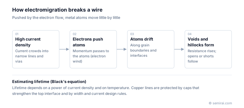
How electromigration damages wires
Electrons colliding with metal atoms push them slowly in the direction of electron flow, an effect often called the electron wind. Atoms move most easily along fast diffusion paths: grain boundaries and the interfaces around the wire. Where atoms leave faster than they arrive, at the cathode end or at a via, a void grows. Where they accumulate, near the anode end, compressive stress builds until metal is pushed out.
The effect depends strongly on current density and temperature. As wires shrink, their cross-section falls faster than the current they carry, so current density rises, and heating from the current itself makes the problem worse. Electromigration is therefore one of the main wear-out mechanisms considered when an interconnect technology is qualified.
Copper interconnects and countermeasures
Aluminium wiring was improved by adding a little copper. Copper, introduced at the end of the 1990s, resists electromigration better than aluminium, but in copper lines the weak point is the top surface, where the copper meets the dielectric cap. Countermeasures therefore focus on that interface: selective metal caps such as cobalt, careful cleaning before capping, and small alloying additions such as manganese.
Designers also follow current-density rules for each wire width and via, add redundant vias, and take advantage of the short-line effect: a line shorter than the Blech length builds up back stress that stops migration.
FAQ
How is electromigration lifetime predicted?
Test structures are stressed at high current density and temperature until a set resistance increase occurs. The failure times are fitted with Black's equation, in which lifetime falls with a power of current density and rises exponentially as temperature falls, and extrapolated to use conditions. JEDEC standard JESD63 describes how to extract these parameters.
Does electromigration also affect solder bumps?
Yes. Flip-chip bumps and microbumps carry large currents through small contacts, and current crowding at the bump corner can cause voids and consumption of the under-bump metal. It is evaluated separately from on-chip wiring.
Is electromigration the same as stress migration?
No. Stress migration moves atoms because of mechanical stress, usually from thermal expansion mismatch, and can create voids even without current. Both are tested during interconnect qualification.
Related pages
Sources
Last updated: November 2, 2026