Gate-All-Around Transistor (GAA)
A gate-all-around (GAA) transistor is a three-dimensional transistor in which the gate electrode wraps the channel on all four sides. FinFETs cover the channel on three sides (tri-gate); a GAA device surrounds nanosheet or nanowire channels completely, which further suppresses short-channel effects and allows lower leakage together with higher drive current.
Also called: GAAFET, all-around gate transistor
Diagram
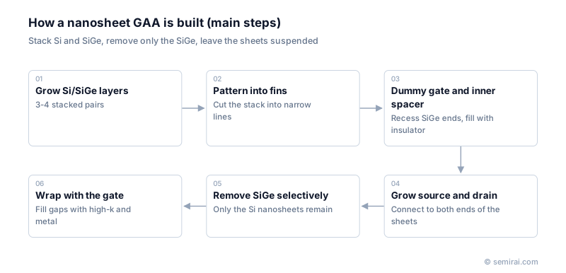
The nanosheet process flow
Building a GAA transistor is mainly a sequence of selective steps. First, three or four pairs of silicon and silicon-germanium (SiGe) layers are grown by epitaxy. The stack is patterned into narrow fins and a temporary dummy gate is formed across them. The ends of the SiGe layers under the dummy gate are recessed sideways and filled with an insulating inner spacer, which later separates the gate from the source and drain. The source and drain are then grown epitaxially, connecting to the ends of the silicon sheets.
Next, the dummy gate is removed and the SiGe is etched away with very high selectivity to silicon, leaving the silicon sheets suspended. Finally, the high-k dielectric and metal gate are deposited by atomic layer deposition into every gap, so that the gate surrounds each sheet. Atomic layer etching (ALE) and ALD precision largely determine device performance and variability.
Adoption and next steps
Samsung was first into production with a 3nm process using its MBCFET in 2022. Intel uses RibbonFET in Intel 18A, and TSMC started volume production of its N2 nanosheet process in the fourth quarter of 2025. Because the effective channel width depends on the number and width of sheets, designers can tune performance and power at the design stage. Research continues on forksheet FETs and complementary FETs (CFET) as the next architectures.
Japanese companies involved
- Rapidus is building a 2nm GAA process at its IIM-1 fab in Chitose, Hokkaido, and reported its first working GAA transistors there in 2025.
- Tokyo Electron supplies etch, deposition and cleaning equipment for steps in this flow, and Kokusai Electric makes batch deposition and ALD systems.
- Rapidus · Leading-edge logic foundry (2 nm, in development)
- Kokusai Electric · Batch deposition, diffusion and ALD equipment
FAQ
Why use SiGe in the stack?
SiGe grows epitaxially on silicon with a matching crystal structure, so it can form clean alternating layers, and it can be etched away much faster than silicon. It acts as a sacrificial spacer that holds the sheets in place until the gate goes in.
What is the inner spacer for?
It insulates the gate metal, which fills the spaces between the sheets, from the source and drain on either side. Without it the gate-to-source/drain capacitance would be large and the device would be slower.
Related pages
Sources
Last updated: November 13, 2026