MBE (Molecular Beam Epitaxy)
MBE (molecular beam epitaxy) grows thin single-crystal films by heating source materials such as gallium and arsenic in ultra-high vacuum, so that they form beams of atoms or molecules aimed at a substrate. The atoms line up with the substrate crystal, and the film grows almost one atomic layer at a time.
Also called: molecular beam epitaxy
Diagram
How MBE works
Each source sits in an effusion cell, also called a Knudsen cell, a heated crucible with a shutter at its opening. Opening and closing the shutters starts and stops each beam. The chamber is held at ultra-high vacuum, around 10⁻⁸ Pa or lower, so the atoms travel to the substrate without colliding with gas molecules.
Growth is slow, on the order of 1 µm per hour, which lets the shutters switch layer composition with single-atomic-layer precision. Reflection high-energy electron diffraction (RHEED) monitors the surface during growth: a beam of electrons strikes the surface at a grazing angle and the diffraction pattern reveals the surface structure.
Where MBE is used
MBE suits devices whose performance depends on atomically abrupt interfaces and very pure layers: quantum wells and superlattices, the channel interface of high-electron-mobility transistors (HEMTs), semiconductor lasers, quantum dots and research on new materials.
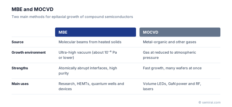
Maintaining ultra-high vacuum takes effort and only a few wafers grow at once, so high-volume production of LEDs and gallium nitride power and RF devices mainly uses metal-organic chemical vapour deposition (MOCVD), which grows faster on many wafers per run.
Japanese companies involved
- EpiQuest is a Japanese maker of molecular beam epitaxy systems for research and production of compound semiconductor films.
- EpiQuest · Molecular beam epitaxy (MBE) systems
FAQ
What is the difference between MBE and MOCVD?
MBE evaporates solid sources in ultra-high vacuum and sends them as beams to the substrate. MOCVD flows metal-organic and hydride gases over a heated substrate, where they react to form the crystal. MBE excels in interface sharpness and purity; MOCVD offers higher growth rates and throughput for mass production.
What do RHEED oscillations show?
During layer-by-layer growth, the intensity of the RHEED pattern rises and falls once for every completed atomic layer, because the surface alternates between smooth and partly covered. Counting the oscillations gives the number of layers grown and the growth rate in real time.
Comparisons
Related pages
- Epitaxy (Epitaxial Growth)
- High Electron Mobility Transistor (HEMT)
- Gallium Arsenide (GaAs)
- Indium Phosphide (InP)
- Quantum Well
- Two-Dimensional Electron Gas (2DEG)
- Vacuum
- Ultra-High Vacuum (UHV)
- Epitaxial growth equipment
- Compound semiconductor equipment
- Canon ANELVA EC8100
- HORIBA PLATO-MicroScan
- Kokusai Electric QUIXACE®-LV
- NuFlare Technology EPIREVO™ S6
Sources
Last updated: November 13, 2026