PN Junction
A pn junction is the boundary formed where p-type and n-type regions meet within a single semiconductor crystal. Carrier diffusion across the boundary leaves a depletion region and a built-in potential barrier, so current flows easily in one direction only. It is the basic building block of diodes, transistors, LEDs, photodiodes and solar cells.
Also called: p-n junction
Diagram
How the depletion region forms
The n side has many free electrons and the p side many holes. Near the boundary, electrons diffuse into the p side and holes into the n side, where they recombine. This leaves the fixed, ionised dopant atoms uncovered: positive donors on the n side and negative acceptors on the p side. Their charge creates an electric field that pushes back against further diffusion, and equilibrium is reached when the two balance.
The carrier-free zone is the depletion region, and the voltage across it is the built-in potential, typically around 0.6–0.9 V in silicon depending on doping. The depletion region extends further into the more lightly doped side and ranges from tens of nanometres to several micrometres wide.
Forward and reverse bias
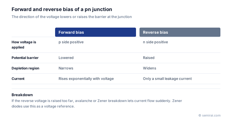
Making the p side positive (forward bias) lowers the barrier, and current rises exponentially with voltage; a silicon diode conducts noticeably from about 0.6–0.7 V. Making the n side positive (reverse bias) raises the barrier and widens the depletion region, so only a small leakage current from thermally generated minority carriers flows. At a high enough reverse voltage the junction breaks down by avalanche multiplication or, in heavily doped junctions, Zener tunnelling.
Because its width changes with voltage, a reverse-biased junction also behaves as a voltage-dependent capacitor, used in varactor diodes and in C-V measurements of doping.
Where pn junctions are used and how they are made
Rectifier diodes use one junction and bipolar transistors two. In a MOSFET the source and drain form junctions with the substrate or well that isolate each transistor. LEDs and laser diodes emit light when injected electrons and holes recombine under forward bias, while photodiodes, image sensors and solar cells use the junction's field to separate carriers created by light. In manufacturing, junctions are formed by ion implantation followed by annealing, by diffusion, or by doping during epitaxial growth. Advanced CMOS needs very shallow, abrupt junctions, achieved with low-energy implants and very short anneals.
Japanese companies involved
- Toshiba and ROHM make discrete diodes, including rectifier, Zener and fast-recovery types, built on pn junctions.
- Sony Semiconductor Solutions makes CMOS image sensors in which a photodiode formed by a pn junction collects light in every pixel.
- Toshiba Electronic Devices & Storage · Power MOSFETs, IGBTs and discrete semiconductors
- ROHM · SiC and silicon power devices, analog ICs
- Sony Semiconductor Solutions · CMOS image sensors
FAQ
How does a pn junction differ from a Schottky junction?
A Schottky junction is formed between a metal and a semiconductor and conducts with majority carriers only. It has a lower forward voltage and switches faster, because no stored minority carriers need to be removed, but it usually leaks more in reverse than a pn junction.
Why does junction leakage matter?
Reverse leakage drains the charge in DRAM cells, appears as dark current in image sensors and adds to standby power. It is mostly caused by defects and metal impurities that create levels in the band gap, so clean, defect-free crystals keep it low.
What sets the breakdown voltage of a junction?
Mainly the doping on the lightly doped side. Lighter doping lets the depletion region spread further, lowering the peak field. Power devices therefore use a thick, lightly doped drift layer to block hundreds or thousands of volts.
Related pages
Sources
Last updated: November 2, 2026