Epitaxy (Epitaxial Growth)
Epitaxy is the growth of a thin single-crystal film on a crystalline substrate so that the film continues the substrate's crystal arrangement and orientation. The name comes from Greek words meaning "arranged upon". Because the layer is grown rather than cut from the bulk, its doping, thickness and even its material can be chosen independently of the substrate.
Also called: epi, epitaxial growth, epitaxial deposition
Diagram
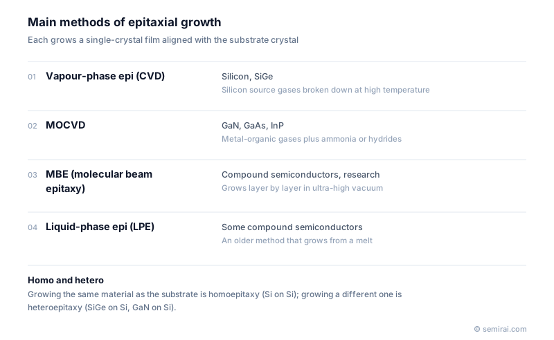
Homoepitaxy and heteroepitaxy
When the film is the same material as the substrate, such as silicon on silicon, the process is called homoepitaxy. The point is usually doping: a lightly doped, defect-free layer can sit on a heavily doped substrate, which is how epitaxial wafers for power MOSFETs and CMOS image sensors are made.
When the film is a different material, the process is heteroepitaxy. Silicon-germanium on silicon and gallium nitride on silicon, sapphire or silicon carbide are common examples. Lattice constants then differ, so the film is either strained to match the substrate or relaxes by forming dislocations. Engineers use the strain deliberately in transistor channels and manage the defects with buffer layers in GaN devices.
Main growth methods
Silicon and SiGe epitaxy is a form of chemical vapour deposition (CVD), often called vapour-phase epitaxy. Silicon-containing gases such as silane or dichlorosilane are decomposed on a hot, carefully cleaned wafer, usually in hydrogen. Compound semiconductors such as GaN, GaAs and InP are mostly grown by metal-organic CVD (MOCVD), which reacts metal-organic sources such as trimethylgallium with ammonia or hydrides. Molecular beam epitaxy (MBE) builds films almost one atomic layer at a time in ultra-high vacuum, mainly for research and specialised devices.
Epitaxy needs an oxide-free starting surface, high purity and tight temperature control. Defect density, doping accuracy and thickness uniformity directly set device performance.
Where epitaxy is used
In CMOS logic, selective epitaxy grows SiGe in the source and drain of p-type transistors to compress the channel and raise hole mobility, while phosphorus-doped silicon is used on the n-type side. Gate-all-around transistors start from a stack of alternating Si and SiGe epitaxial layers. Silicon carbide power devices rely on thick, lightly doped epitaxial drift layers, and LEDs, lasers and GaN power and RF transistors are built entirely from epitaxial layers.
Japanese companies involved
- Shin-Etsu Chemical and SUMCO make silicon epitaxial wafers for logic, image sensors and power devices.
- NuFlare Technology makes epitaxial growth reactors, including systems for silicon carbide, and Taiyo Nippon Sanso makes MOCVD equipment for compound semiconductors.
- Shin-Etsu Chemical · Silicon wafers, photoresists and photomask blanks
- SUMCO · Silicon wafers
- NuFlare Technology · Electron-beam mask writers, mask inspection and epitaxial reactors
- Taiyo Nippon Sanso · Specialty gases, gas supply systems and MOCVD equipment
FAQ
What is the difference between epitaxy and ordinary CVD?
Epitaxy is a special case of CVD. Ordinary CVD can deposit amorphous or polycrystalline films on any surface, while epitaxy produces only single-crystal material that follows the substrate. That demands higher temperatures or very clean surfaces, purer gases and stricter control than most deposition steps.
What is selective epitaxial growth?
Selective epitaxy grows crystal only on exposed silicon and not on nearby oxide or nitride. Adding a chlorine-containing gas such as HCl etches away nuclei that start on the dielectric, so the film forms only where it is wanted, for example in source and drain regions.
Why are power devices built on epitaxial layers?
The voltage a power device can block depends on the thickness and doping of its drift layer. Epitaxy lets makers grow a precisely controlled, lightly doped layer on a heavily doped, low-resistance substrate, combining high breakdown voltage with low on-resistance.
Comparisons
Related pages
Sources
Last updated: November 2, 2026