Line Edge Roughness (LER)
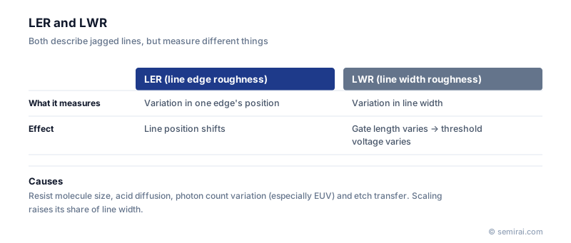
Line edge roughness (LER) is the nanometre-scale jaggedness by which the edge of a pattern formed by lithography and development deviates from an ideal straight line. The related variation in the width of a line is called line width roughness (LWR). As features shrink, the same few nanometres of roughness become a larger fraction of the line width.
Also called: LER, line width roughness, LWR
Diagram
Where the roughness comes from
The resist is made of molecules and polymer chains of finite size, and the photoacid generators and other components are not perfectly evenly distributed. In chemically amplified resists, acid diffusion during baking blurs and randomises the edge. Development dissolves the polymer unevenly at the molecular scale.
In EUV lithography, photon shot noise adds to these causes: because few photons are absorbed per unit area, the local dose varies randomly along the edge. Etching can smooth some roughness or transfer it to the final structure, so the roughness after etch is what ultimately matters.
Effects and measurement
In a transistor gate, LWR means the gate length varies along the width of the device, causing variation in threshold voltage and drive current and raising leakage where the gate is shortest. In interconnects, roughness raises resistance variation and can reduce reliability.
LER and LWR are usually measured with a critical-dimension scanning electron microscope (CD-SEM) and reported as three standard deviations (3σ) of edge or width position, sometimes with analysis of how the roughness is distributed across spatial frequencies. Because SEM images are noisy, measurement noise has to be separated from true roughness.
Japanese companies involved
- JSR, Tokyo Ohka Kogyo (TOK) and Shin-Etsu Chemical develop resists designed to reduce roughness at advanced nodes.
- Hitachi High-Tech makes CD-SEMs widely used to measure line width and roughness in fabs.
- Hitachi High-Tech · CD-SEM metrology, defect inspection and etch systems
- JSR · Photoresists and semiconductor materials
- Tokyo Ohka Kogyo (TOK) · Photoresists and high-purity process chemicals
- Shin-Etsu Chemical · Silicon wafers, photoresists and photomask blanks
FAQ
What is the difference between LER and LWR?
LER describes the variation of one edge's position; LWR describes variation of the line width, the distance between the two edges. If the two edges vary independently, LWR is about √2 times LER.
Why is LER a problem?
It makes the effective dimension of a device vary from place to place. For gates this shows up as threshold voltage variation, and because roughness does not shrink as fast as line width, its relative impact grows at each node.
How is LER reduced?
With resist chemistry that reacts more uniformly, such as metal-oxide resists, with higher exposure dose to reduce shot noise, with post-development smoothing and with etch processes that smooth edges. Higher dose lowers throughput, so the improvement must be traded against productivity.
Related pages
Sources
Last updated: November 2, 2026