Lithography Equipment
Lithography equipment is the tool that transfers the circuit pattern on a photomask onto the photoresist coating a wafer, using ultraviolet light or, in some tools, an electron beam. It turns a chip design into a physical pattern, and its resolution sets the finest features, and therefore the most advanced process generation, a fab can produce.
Also called: exposure tool, scanner, stepper, lithography system
Diagram
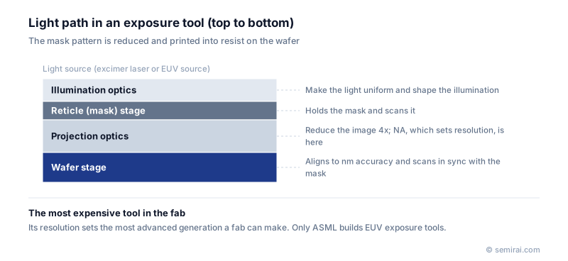
How a scanner is built
A modern exposure tool is a stack of precision subsystems along one light path. A light source (an excimer laser for deep ultraviolet, or a tin-plasma source for extreme ultraviolet) feeds an illumination system that makes the light uniform and gives it a chosen angular shape. The light passes through, or reflects off, the reticle, and projection optics shrink the image, usually by four times, onto the wafer.
Most production tools today are scanners: the reticle stage and the wafer stage move in opposite directions in perfect synchronisation while a slit of light sweeps across each field. The wafer stage must position every field to within a few nanometres of the layers already on the wafer, so stage control and alignment are as important as the optics.
What limits resolution
The smallest printable feature follows the Rayleigh relation R = k₁ × λ / NA, where λ is the wavelength, NA the numerical aperture of the projection optics and k₁ a factor that reflects how aggressive the process is. Lithography has advanced by shortening the wavelength (i-line at 365 nm, KrF at 248 nm, ArF at 193 nm, EUV at 13.5 nm), by raising NA (including water immersion for ArF) and by lowering k₁ with optical proximity correction, off-axis illumination and source-mask optimisation.
Deep ultraviolet (DUV) tools use refractive lenses. Extreme ultraviolet (EUV) light is absorbed by glass and air, so EUV tools use multilayer mirrors inside a vacuum. When a single exposure cannot resolve a pattern, chipmakers split it across several exposures and etches (multi-patterning), at the cost of more process steps.
Japanese companies involved
- Nikon makes ArF immersion, ArF dry, KrF and i-line scanners and steppers for front-end chip production.
- Canon makes i-line and KrF steppers and scanners, including tools for advanced packaging, and develops nanoimprint lithography as an alternative patterning method.
- Gigaphoton supplies KrF and ArF excimer lasers used as light sources in DUV exposure tools.
- Gigaphoton · Excimer laser light sources for lithography
- Nikon · ArF, KrF and i-line lithography systems
- Canon · Lithography steppers and nanoimprint lithography
FAQ
Who makes EUV lithography tools?
Only ASML in the Netherlands builds EUV scanners for volume production. In DUV lithography ASML, Nikon and Canon all compete, with Canon concentrating on i-line and KrF tools.
What is the difference between a stepper and a scanner?
A stepper exposes a whole field at once and then steps to the next one. A scanner exposes the field through a narrow slit while moving the reticle and wafer together, which allows a larger field with a smaller, better-corrected lens. Leading-edge front-end layers are printed on scanners.
Why is lithography the most critical step in chipmaking?
Every patterned layer, often dozens per chip, passes through lithography, and the overlay between layers must be controlled to a few nanometres. The resolution and overlay of the exposure tool therefore limit both how small a transistor can be and how well the layers line up.
Related pages
Sources
Last updated: November 2, 2026