Oxide Film (Silicon Dioxide)
In semiconductor manufacturing, an oxide film usually means silicon dioxide (SiO₂), an excellent insulator with a band gap of about 9 eV. It is either grown by heating silicon in oxygen or steam (thermal oxide) or deposited from precursors such as TEOS (CVD oxide), and is used for gate dielectrics, isolation, interlayer dielectrics and hard masks.
Also called: silicon oxide, SiO₂, thermal oxide, CVD oxide
Diagram
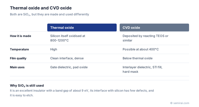
Thermal oxide and CVD oxide
Thermal oxide is grown in an oxidation furnace at roughly 800-1200°C, either in dry oxygen or in steam (wet oxidation, which is faster). The silicon itself is consumed to form the oxide: about 44% of the final film thickness lies below the original silicon surface. The film is dense and the Si/SiO₂ interface has very few defects, so thermal oxide is used where quality matters most, such as gate oxides and pad oxides.
CVD oxide is deposited from TEOS or silane at temperatures down to about 400°C. It can be made thick on any underlying material, so it is used for interlayer dielectrics (undoped NSG and doped BPSG), shallow trench isolation (STI) fill and hard masks. Silicon left in air also grows a native oxide about 1-2 nm thick.
Why SiO₂ made silicon dominant
Silicon can be turned into a high-quality, stable insulator just by heating it, and that insulator forms a nearly perfect interface with the crystal. Few other semiconductors have such a convenient native oxide, which is one of the main reasons silicon became the material of the electronics industry.
Gate oxides were thinned with each generation until, at around 1 nm, tunnelling leakage became too large. From the 45 nm generation onwards, leading-edge logic replaced the gate oxide with high-k dielectrics such as HfO₂, and gate dielectrics are now compared by equivalent oxide thickness (EOT). A very thin SiO₂ layer still sits beneath the high-k film as the interfacial layer.
Japanese companies involved
- Kokusai Electric and Tokyo Electron make batch vertical furnaces used for thermal oxidation and for depositing oxide films.
- Tokyo Electron (TEL) · Coat/develop, etch and deposition equipment
- Kokusai Electric · Batch deposition, diffusion and ALD equipment
FAQ
Why does CVD oxide etch faster than thermal oxide?
CVD oxide is less dense and can contain hydrogen, hydroxyl groups or carbon from the precursor. In hydrofluoric acid it therefore etches faster than thermal oxide, and the ratio of etch rates is often used as a quick check of CVD film quality and densification.
How is oxide removed?
Wet processes use dilute hydrofluoric acid (DHF) or buffered HF (BHF). Dry processes use plasmas of fluorine-containing gases such as CF₄ or C₄F₈. The native oxide is normally stripped with dilute HF right before deposition or epitaxial growth.
How is oxide thickness measured?
Ellipsometry and optical interference (reflectometry) tools measure it quickly and without contact. They rely on the well-known refractive index of SiO₂, about 1.46, and are used for routine monitoring on production wafers.
Related pages
- Gate Oxide (Gate Dielectric)
- Native Oxide
- TEOS (Tetraethyl Orthosilicate)
- EOT (Equivalent Oxide Thickness)
- Insulating Film (Dielectric Film)
- Shallow Trench Isolation (STI)
- BPSG / PSG (Borophosphosilicate Glass)
- LOCOS (Local Oxidation of Silicon)
- Oxidation furnaces
- CVD equipment
- Kokusai Electric QUIXACE®
- Kokusai Electric QUIXACE®-II
- Kokusai Electric QUIXACE ULTIMATE®
- Kokusai Electric VERTEX Revolution
Sources
Last updated: November 13, 2026