Panel-Level Packaging (PLP)
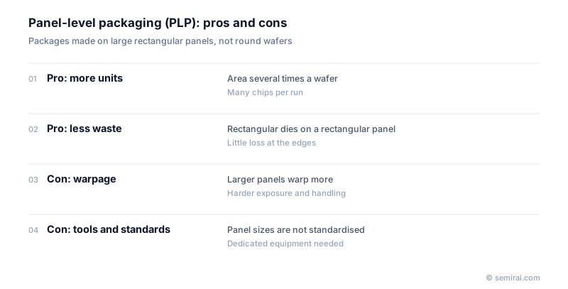
Panel-level packaging (PLP) is a way of carrying out wafer-level-style packaging processes, especially fan-out packaging, on large rectangular panels instead of 300 mm round wafers. A panel holds several times the area of a wafer, so more packages are processed in each step and less area is lost at the edges.
Also called: fan-out panel-level packaging, FOPLP
Diagram
How it works and why it saves cost
In fan-out packaging, tested dies are placed on a carrier, embedded in mold compound and covered with redistribution layers (RDL) that route their connections outwards, before solder balls are attached and the carrier is cut into individual packages. PLP does the same on rectangular panels several hundred millimetres on a side, borrowing equipment ideas from printed circuit board and flat-panel display manufacturing.
Rectangular dies fit a rectangular panel with little waste, whereas a round wafer leaves partial sites around the edge. The larger area also means each lithography, plating or molding step handles more packages. For large packages, such as AI processors with several chiplets, only a handful fit on a 300 mm wafer, which makes panels especially attractive.
Technical challenges
Large thin panels warp, especially after molding, which makes handling, alignment and lithography harder. Keeping film thickness, plating and exposure uniform over the whole panel is difficult, and dies can shift slightly during molding, so lithography must correct for their positions. Panel sizes are not yet standardised, so equipment makers must design tools for several formats and cannot simply reuse wafer tools.
Glass carriers and glass core substrates are often discussed together with PLP because their flatness helps with fine RDL patterning.
Japanese companies involved
- Resonac has organised a consortium of Japanese and overseas materials and equipment companies to develop panel-level organic interposers.
- TOWA and other Japanese back-end equipment makers supply compression molding equipment of the kind used to encapsulate dies on large carriers.
- Resonac · CMP slurries, packaging materials and SiC epitaxial wafers
- TOWA · Molding (encapsulation) equipment for chip packaging
- Tokyo Seimitsu (ACCRETECH) · Wafer probers, dicing and grinding machines, metrology
FAQ
How is PLP different from FOWLP?
The process steps are similar; the difference is the carrier. Fan-out wafer-level packaging (FOWLP) uses a round reconstituted wafer that fits existing wafer tools, while PLP uses a rectangular panel that needs new or adapted equipment but gives more area per run.
Is panel-level packaging in mass production?
Yes for some smaller fan-out packages, for example power management and mobile chips. Using panels for large, fine-pitch AI packages is still under development, with several foundries and OSATs building pilot lines.
Related pages
Sources
Last updated: November 13, 2026