Printed Circuit Board (PCB)
A printed circuit board (PCB) is a board with copper wiring on and inside an insulating base, on which semiconductor packages and passive components are mounted and connected. Also called a printed wiring board (PWB), it is the foundation of almost all electronics. A board with components soldered on is often called a PCBA (printed circuit board assembly).
Also called: printed wiring board, PWB, PCBA
Diagram
How a PCB is made
Fabrication starts from copper clad laminate (CCL), usually glass cloth impregnated with epoxy. The copper foil is etched into wiring, and holes are drilled and plated with copper to connect the layers.
Boards range from single- and double-sided boards to multilayer boards with dozens of layers and HDI (high-density interconnect) boards that stack fine lines and small laser-drilled vias. Flexible boards use polyimide films. The standard rigid material is FR-4 glass-epoxy, while high-speed equipment uses special low-loss materials.
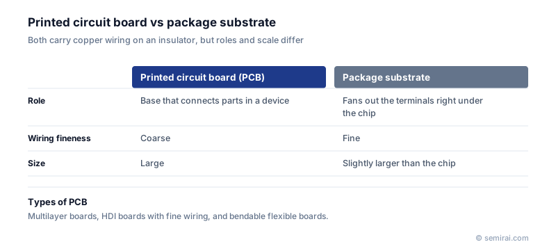
PCB vs package substrate
Both are wiring boards, but their roles and scale differ. A package substrate sits directly under the chip and fans out the chip's very fine pad pitch to a spacing that can be soldered to a PCB. Its line widths run from a few micrometres to a few tens of micrometres, far finer than typical PCB lines of tens of micrometres and more.
Packages are attached to the PCB by surface mounting: solder balls or leads are placed on solder paste and joined in a reflow oven.
Japanese companies involved
- IBIDEN and Shinko Electric Industries are major makers of package substrates, the fine-pitch boards between chip and PCB.
- Resonac supplies laminates, prepregs and other materials used to fabricate printed circuit boards.
- IBIDEN · IC package substrates (FC-BGA)
- Shinko Electric Industries · FC-BGA package substrates and lead frames
- Resonac · CMP slurries, packaging materials and SiC epitaxial wafers
FAQ
Why are most boards green?
The colour comes from the solder resist, the protective coating over the copper, not from the board itself. Green became the industry convention, but resist is also available in black, white, blue and red; white is often used on LED boards for its reflectivity.
What does HDI mean?
HDI stands for high-density interconnect. These boards use thin dielectric layers, fine lines and small laser-drilled microvias stacked layer on layer, so that many connections fit into a small area. Smartphone main boards are a typical example.
Related pages
- Copper Clad Laminate (CCL)
- Package Substrate
- Surface Mount Technology (SMT)
- BGA (Ball Grid Array)
- Reflow Soldering
- Solder Ball
- ABF (Ajinomoto Build-up Film)
- FR-4
- Package substrates (FC-BGA)
- IBIDEN FC-BGA substrates
- Shinko Electric Industries DLL® / DLL3® (flip-chip package substrates)
- Ajinomoto ABF GL-102
- Ajinomoto ABF GX-92
Sources
Last updated: November 12, 2026