Phonon
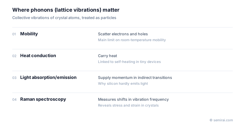
A phonon is a quantum of lattice vibration, the collective motion of atoms in a crystal treated as if it were a particle. In semiconductors, phonons scatter electrons and holes and are a main limit on mobility at room temperature. They also carry heat and take part in light absorption and emission in indirect-bandgap materials such as silicon.
Also called: lattice vibration, phonon scattering
Diagram
What phonons are
The atoms of a crystal are bound to their neighbours as if by springs, so a vibration travels through the lattice as a wave whose energy comes in discrete amounts. The name comes from the Greek for sound, by analogy with the photon, the quantum of light. In acoustic phonons neighbouring atoms move in the same direction; in optical phonons they move in opposite directions.
Heat in a semiconductor is carried mainly by phonons. Silicon conducts heat well, about 150 W/m·K at room temperature, which is one reason it makes a good substrate.
Effects on devices and measurement
Electrons and holes collide with phonons and change direction. As temperature rises there are more phonons, so mobility falls. In silicon a photon cannot move an electron across the gap alone because the band edges sit at different momenta; a phonon must supply the missing momentum, which is why silicon absorbs weakly near its band edge and hardly emits light.
In nanoscale transistors and nanosheets, phonon scattering at surfaces and interfaces makes heat harder to remove, so self-heating degrades performance and reliability. With high-k gate dielectrics, vibrations in the insulator can scatter channel electrons (remote phonon scattering) and lower mobility.
Raman spectroscopy uses the small shift in wavelength when light exchanges energy with optical phonons. Silicon has a Raman peak at about 520 cm⁻¹, and the shift of that peak reveals stress and strain in the crystal without damaging it.
Japanese companies involved
- HORIBA makes Raman spectrometers that are used to measure stress and strain in silicon and other semiconductor materials.
- HORIBA · Mass flow controllers and process monitoring instruments
FAQ
Why does mobility fall as temperature rises?
Higher temperature excites more lattice vibrations, so carriers meet phonons more often and travel shorter distances between collisions. In lightly doped silicon near room temperature, phonon scattering dominates; at low temperature or high doping, scattering by ionised impurities becomes more important.
Why does stress shift the Raman peak?
Strain changes the distance between atoms and so the stiffness of their bonds. That changes the frequency of the optical phonon, and the scattered light shifts with it. Compressive stress moves the silicon peak up and tensile stress moves it down.
Related pages
Sources
Last updated: November 2, 2026