Raman Spectroscopy
Raman spectroscopy shines laser light on a material and measures the small fraction of scattered light that has changed wavelength by exchanging energy with atomic vibrations (phonons). The size of this change, the Raman shift, depends on bond strength and crystal structure, so the spectrum acts like a fingerprint of the material and its condition.
Also called: Raman, micro-Raman, Raman stress measurement
Diagram
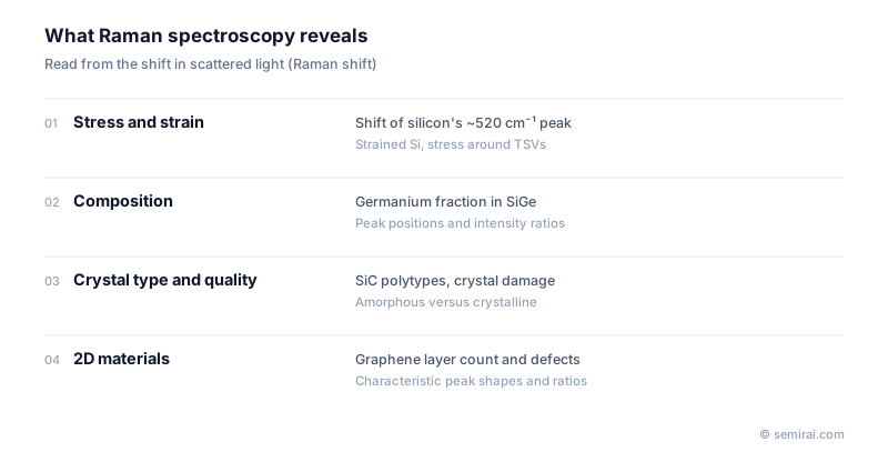
Measuring stress in silicon
The most common semiconductor use is stress measurement. Crystalline silicon has a sharp Raman peak at about 520 cm⁻¹. Tensile strain moves the peak to lower wavenumbers and compressive strain to higher ones, so the shift indicates the size and sign of the stress. This is used to study strained silicon channels and the stress around trenches, shallow trench isolation and through-silicon vias (TSVs).
Because the laser can be focused to about a micrometre, a micro-Raman system can scan a sample and draw a map of stress. Converting the shift into stress requires a coefficient that depends on the material and crystal orientation, so quantitative work needs care.
Other uses, strengths and limits
Raman also measures the germanium fraction in SiGe, identifies SiC polytypes and crystal damage, counts graphene layers and their defects, and distinguishes amorphous from crystalline silicon, for instance after laser annealing. It needs no vacuum and no sample preparation, and it does not damage the sample at normal laser power.
Raman scattering is very weak, so samples that fluoresce strongly can hide the signal, and too much laser power can heat the sample and shift its peaks. The probing depth also depends on the laser wavelength, so ultraviolet lasers are chosen when only the top layer of silicon should be measured.
Japanese companies involved
- HORIBA and JASCO make Raman spectrometers and Raman microscopes used to evaluate stress, composition and crystal quality in semiconductor materials.
FAQ
What is the difference between Raman and infrared spectroscopy?
Both probe molecular and lattice vibrations, but infrared measures light absorbed directly by vibrations that change a dipole moment, while Raman measures scattered light from vibrations that change polarisability. The two often see different vibrations, so they complement each other.
Is a Raman shift a wavelength?
No. It is the energy difference between the laser and the scattered light, expressed in wavenumbers (cm⁻¹). Because it is a difference, the same material gives the same Raman shift whatever laser wavelength is used.
Related pages
Sources
Inspection and metrology terms
Last updated: November 13, 2026