Quantum Well
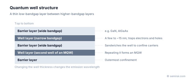
A quantum well is a thin layer of a narrow-bandgap semiconductor sandwiched between layers with a wider bandgap, which confines electrons and holes inside the thin layer. The well is typically a few nanometres to a little over ten nanometres thick. On an energy diagram it looks like a dip, or well, in which the carriers sit.
Also called: multiple quantum well, MQW
Diagram
Quantised energy levels
When the layer becomes about as thin as the wavelength of an electron, quantum mechanics restricts the energies the electron can have to discrete levels. Those levels depend on the well thickness, so the emission wavelength can be tuned by changing the thickness without changing the material.
Confining electrons and holes in the same narrow region also makes them more likely to meet and recombine radiatively, which raises light-emission efficiency. A quantum well can be seen as two heterojunctions facing each other, using the band offsets to trap carriers.
Use in LEDs and lasers
Quantum wells form the active layer of most semiconductor lasers and LEDs. Several wells stacked with barrier layers between them, called a multiple quantum well (MQW), are common. Blue and white LEDs emit light from InGaN/GaN multiple quantum wells.
In lasers, quantum wells lower the threshold current and improve efficiency and temperature behaviour. Growing layers only a few nanometres thick with atomic-scale control requires crystal growth methods such as molecular beam epitaxy (MBE) and metal-organic chemical vapour deposition (MOCVD).
Japanese companies involved
- Nichia makes GaN-based LEDs and laser diodes whose light comes from InGaN quantum well active layers.
- Sumitomo Electric Industries supplies compound semiconductor substrates such as GaAs and InP used for growing quantum well devices.
- Nichia · LEDs and laser diodes
- Sumitomo Electric Industries (compound semiconductors) · SiC epitaxial wafers and GaAs and InP substrates
FAQ
Why use multiple quantum wells instead of one?
A single well can hold only a limited number of carriers before it fills up. Stacking several wells increases the volume that emits light, which raises brightness and efficiency at higher currents. The number of wells and barrier thickness are chosen for each device.
How are quantum wells related to quantum wires and quantum dots?
A quantum well confines carriers in one direction, leaving them free to move in a plane. A quantum wire confines them in two directions and a quantum dot in all three. Quantum dots are used in some lasers and in display colour conversion.
Related pages
Sources
Last updated: November 2, 2026