Thermal Via
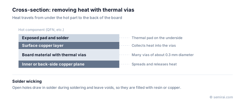
A thermal via is a copper-plated hole in a printed circuit board or package substrate whose purpose is to conduct heat rather than electrical signals. It is built like an ordinary via, but it is placed to move heat quickly from a hot component to inner copper layers or to the far side of the board.
Also called: thermal vias, heat-dissipation via
Diagram
Why boards need them
Board materials such as glass-epoxy are poor conductors of heat, so heat builds up under a hot component unless it is given a path out. Packages such as QFN have an exposed thermal pad on their underside for this reason.
An array of vias is placed directly beneath that pad, often around 0.3 mm in diameter at roughly 1 mm pitch, using copper's high thermal conductivity to carry heat to inner or back-side copper planes. More vias, and vias filled with copper, conduct more heat.
Solder wicking and other design points
Open vias cause a problem during soldering: molten solder can be drawn down into the holes, leaving voids in the joint or too little solder under the pad. Vias are therefore filled with resin or copper and capped, or covered with solder resist.
The vias are usually tied to a large ground plane that spreads the heat. The same idea appears in 3D chip stacking, where through-silicon vias dedicated to heat removal, sometimes called thermal TSVs, are being studied.
Japanese companies involved
- IBIDEN and Shinko Electric Industries manufacture package substrates, where filled and stacked vias provide both electrical and thermal paths beneath the chip.
- IBIDEN · IC package substrates (FC-BGA)
- Shinko Electric Industries · FC-BGA package substrates and lead frames
FAQ
How is a thermal via different from a normal via?
The construction is the same, a copper-plated hole. The difference is purpose: a normal via connects signal or power between layers, while a thermal via is placed in clusters under a hot component and connected to large copper areas to spread heat.
Does via diameter matter?
Yes, but in balance. Larger vias carry more heat individually, but they make solder wicking worse and take more space. Designers often prefer many smaller vias, filled where possible, over a few large ones.
Related pages
Sources
Last updated: November 12, 2026