Photoluminescence (PL)
Photoluminescence (PL) is light emitted by a semiconductor after it absorbs light with energy above its band gap: the excited electrons and holes recombine and release photons characteristic of the material. Measuring the wavelength and intensity of this light gives a contactless, non-destructive way to check composition, crystal quality and defects.
Also called: PL, PL spectroscopy, PL imaging
Diagram
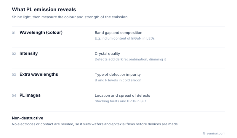
What PL reveals
The emission wavelength reflects the band gap, so PL is used to check the composition of compound semiconductors, for example the indium content of InGaN layers in LEDs. The intensity and width of the emission reflect crystal quality: defects and impurities provide paths for non-radiative recombination, which weakens the light, and some defects emit at their own characteristic wavelengths.
For silicon, which emits only weakly because its band gap is indirect, low-temperature PL with the sample cooled to liquid helium temperature can measure very low concentrations of dopants such as boron and phosphorus from their characteristic emission lines.
PL imaging for wafer inspection
PL imaging captures the emission across a whole wafer and has become a standard inspection method. In silicon carbide (SiC), basal plane dislocations and stacking faults, which can degrade power devices, appear as distinct lines and triangles in PL images, so substrates and epitaxial layers are screened this way. In silicon, PL maps show the spread of carrier lifetime and metal contamination.
Japanese companies involved
- HORIBA and Hamamatsu Photonics make photoluminescence measurement instruments used to evaluate semiconductor materials.
- Lasertec makes SiC wafer inspection and review systems used to find crystal defects in substrates and epitaxial layers.
- Lasertec · EUV mask and mask blank inspection
- HORIBA · Mass flow controllers and process monitoring instruments
- Hamamatsu Photonics · Failure analysis, process monitoring and static elimination equipment
FAQ
How is PL different from electroluminescence?
Both come from electron-hole recombination. In PL the carriers are created by light; in electroluminescence (EL) they are injected by an electric current, as in an operating LED. PL needs no electrodes, so it can be used on bare wafers and films before any device is made.
Does PL damage the sample?
Normally not. The excitation is a modest laser beam, so the wafer can continue through processing. Very high laser power can heat a small spot, so power is chosen to give enough signal without changing the material.
Related pages
- Band Gap
- SiC Wafer (Silicon Carbide Substrate)
- Gallium Nitride (GaN)
- Metal Contamination
- Raman Spectroscopy
- Wafer substrate inspection equipment
- Kobelco Research Institute EPM-2200
- Kobelco Research Institute LEP series
- Kobelco Research Institute LTA-2200EP/F
- Kobelco Research Institute SBW series flatness and shape measurement systems
Sources
Last updated: November 13, 2026