Yield Management
Yield management is the organised process a semiconductor fab uses to raise yield, the share of good dies per wafer. It combines defect inspection, process and equipment data, electrical test and failure analysis to locate where yield is lost, trace each loss to a root cause and feed the fix back into the process.
Also called: yield enhancement, yield management system (YMS)
Diagram
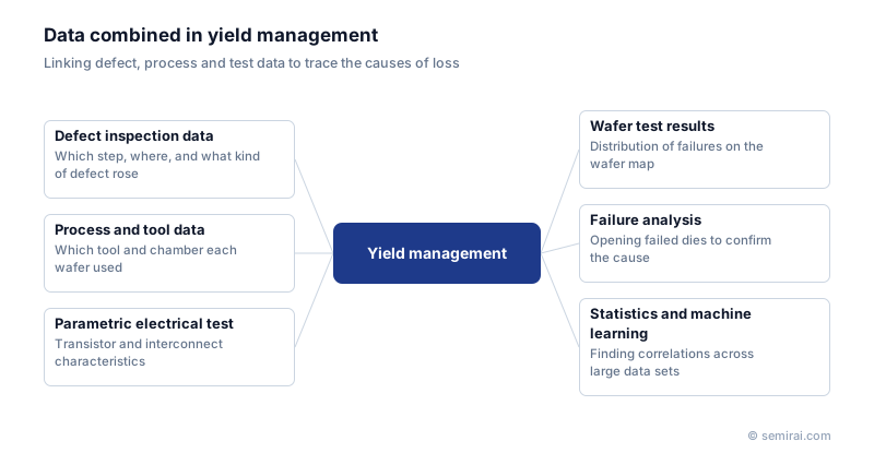
How yield is lost and how it is traced
Yield loss has two broad sources. Random defects, such as particles and scratches, kill dies at scattered locations; their effect depends on defect density and die area. Systematic losses come from the process or design itself, for example a lithography hotspot, a drifting chamber or a pattern that etches poorly, and they repeat in recognisable patterns.
The work follows a loop. Inline inspection tools scan wafers after key steps and report where defect counts rise. Review SEMs image the defects and classify them, increasingly with machine-learning image classifiers. Engineers then look at wafer maps from probe test: a ring at the edge, a cluster in one quadrant or a repeating reticle pattern each suggest different causes. Linking those maps with the tool and chamber each wafer passed through narrows the suspects, and failure analysis of failing dies confirms the mechanism. The fix goes back as a recipe change, a maintenance action or new control limits in statistical process control (SPC) and advanced process control (APC).
Yield management systems
Because a modern fab produces huge volumes of inspection, metrology, equipment-sensor and test data, the analysis runs on a yield management system (YMS): a database and software layer that joins all of it by lot, wafer and die. Equipment makers and software companies such as KLA, Applied Materials, PDF Solutions and Synopsys offer such platforms. The value lies less in any single data source than in being able to correlate them quickly.
Why it matters
In a new process node, yield starts low and rises over months of learning. How fast that ramp proceeds decides when the node becomes profitable, so yield learning speed is one of a fab's main competitive measures. In mature production, small yield gains translate directly into lower cost per good die, since the cost of processing a wafer is almost fixed.
Japanese companies involved
- Hitachi High-Tech makes defect review SEMs, wafer inspection systems and CD-SEMs whose data feed yield analysis in fabs.
- Hitachi High-Tech · CD-SEM metrology, defect inspection and etch systems
FAQ
What is the difference between yield management and quality control?
Quality control checks that shipped products meet specification. Yield management works earlier, inside the fab, to cut the number of dies that fail at all. The two share data, but yield management is aimed at cost and learning speed rather than at screening out bad parts.
What is a killer defect?
A defect large enough, and in the wrong place, to make a die fail, for example a particle that bridges two lines. Many detected defects are harmless, so classification aims to separate killer defects from nuisance ones and to focus attention on the steps that create the former.
What is a yield model?
A formula that estimates die yield from defect density and die area, such as the Poisson or negative binomial models. It explains why large dies yield worse than small ones on the same process and helps set defect density targets for each layer.
Related pages
Sources
Last updated: November 2, 2026